

Question
We will add these codes to the program 1)------------- AND Gate for Partial Product Generator-------- --Purpose: AND gate used in partial product Generator --Style of
We will add these codes to the program 1)------------- AND Gate for Partial Product Generator-------- --Purpose: AND gate used in partial product Generator --Style of modelling: Dataflow library IEEE; use IEEE.STD_LOGIC_1164.ALL; use IEEE.STD_LOGIC_ARITH.ALL; use IEEE.STD_LOGIC_UNSIGNED.ALL;
entity myAND is Port ( a : in STD_LOGIC; b : in STD_LOGIC; Y : out STD_LOGIC); end myAND; architecture Behavioral of myAND is begin Y
2)----------Full Adder-----------
--Style of Modelling: Dataflow
library IEEE; use IEEE.STD_LOGIC_1164.ALL; entity fullAdder is Port ( A : in STD_LOGIC; B : in STD_LOGIC; Cin : in STD_LOGIC; S : out STD_LOGIC; Cout : out STD_LOGIC); end fullAdder; architecture fulladd of fullAdder is signal AxorB: std_logic; signal NotA, NotB, NotCin: std_logic; signal t1, t2, t3, t4: std_logic; signal AandB, BandCin, AandCin: std_logic; begin -- AxorB
3)------------ 8 Bit Array Multiplier ------------------ --Purpose: Design of 8 Bit Array multiplier using partial product generator and mapping Full adders. --Style of modelling: Structural library IEEE; use IEEE.STD_LOGIC_1164.ALL; use IEEE.STD_LOGIC_ARITH.ALL; use IEEE.STD_LOGIC_UNSIGNED.ALL;
entity multi_8bit is Port ( a : in STD_LOGIC_VECTOR (7 downto 0); x : in STD_LOGIC_VECTOR (7 downto 0); p : out STD_LOGIC_VECTOR (15 downto 0)); end multi_8bit;
architecture Behavioral of multi_8bit is --- Component Declaration
component creating_pp port(a,b : in std_logic_vector(7 downto 0);y: out std_logic_vector(63 downto 0)); end component;
component fullAdder port (a,b,cin:in STD_LOGIC; s,cout:out STD_LOGIC); end component;
--- Signal Declaration signal y :STD_LOGIC_VECTOR (63 downto 0); signal cf :STD_LOGIC_VECTOR (59 downto 0); signal S :STD_LOGIC_VECTOR (55 downto 0); begin p1: creating_pp port map(a,x,y); -- first number, second, partials p(0)
4)----------- Partial Product Generator for Multiplier --------- --Purpose: Generation of 64 (8x8) partial products for input operands. --Style of modelling: Structural library IEEE; use IEEE.STD_LOGIC_1164.ALL; use IEEE.STD_LOGIC_ARITH.ALL; use IEEE.STD_LOGIC_UNSIGNED.ALL;
entity creating_pp is Port ( A : in STD_LOGIC_VECTOR (7 downto 0); B : in STD_LOGIC_VECTOR (7 downto 0); Y : out STD_LOGIC_VECTOR (63 downto 0)); end creating_pp; architecture Behavioral of creating_pp is -- component declaration component myAND port(a,b : in std_logic; y: out std_logic); end component; begin a0: myAND port map(a(0),b(0),y(0));a1: myAND port map(a(1),b(0),y(1)); a2: myAND port map(a(2),b(0),y(2));a3: myAND port map(a(3),b(0),y(3)); a4: myAND port map(a(4),b(0),y(4));a5: myAND port map(a(5),b(0),y(5)); a6: myAND port map(a(6),b(0),y(6));a7: myAND port map(a(7),b(0),y(7)); a8: myAND port map(a(0),b(1),y(8));a9: myAND port map(a(1),b(1),y(9)); a10: myAND port map(a(2),b(1),y(10));a11: myAND port map(a(3),b(1),y(11)); a12: myAND port map(a(4),b(1),y(12));a13: myAND port map(a(5),b(1),y(13)); a14: myAND port map(a(6),b(1),y(14));a15: myAND port map(a(7),b(1),y(15)); a16: myAND port map(a(0),b(2),y(16));a17: myAND port map(a(1),b(2),y(17)); a18: myAND port map(a(2),b(2),y(18));a19: myAND port map(a(3),b(2),y(19)); a20: myAND port map(a(4),b(2),y(20));a21: myAND port map(a(5),b(2),y(21)); a22: myAND port map(a(6),b(2),y(22));a23: myAND port map(a(7),b(2),y(23)); a24: myAND port map(a(0),b(3),y(24));a25: myAND port map(a(1),b(3),y(25)); a26: myAND port map(a(2),b(3),y(26));a27: myAND port map(a(3),b(3),y(27)); a28: myAND port map(a(4),b(3),y(28));a29: myAND port map(a(5),b(3),y(29)); a30: myAND port map(a(6),b(3),y(30));a31: myAND port map(a(7),b(3),y(31)); a32: myAND port map(a(0),b(4),y(32));a33: myAND port map(a(1),b(4),y(33)); a34: myAND port map(a(2),b(4),y(34));a35: myAND port map(a(3),b(4),y(35)); a36: myAND port map(a(4),b(4),y(36));a37: myAND port map(a(5),b(4),y(37)); a38: myAND port map(a(6),b(4),y(38));a39: myAND port map(a(7),b(4),y(39)); a40: myAND port map(a(0),b(5),y(40));a41: myAND port map(a(1),b(5),y(41)); a42: myAND port map(a(2),b(5),y(42));a43: myAND port map(a(3),b(5),y(43)); a44: myAND port map(a(4),b(5),y(44));a45: myAND port map(a(5),b(5),y(45)); a46: myAND port map(a(6),b(5),y(46));a47: myAND port map(a(7),b(5),y(47)); a48: myAND port map(a(0),b(6),y(48));a49: myAND port map(a(1),b(6),y(49)); a50: myAND port map(a(2),b(6),y(50));a51: myAND port map(a(3),b(6),y(51)); a52: myAND port map(a(4),b(6),y(52));a53: myAND port map(a(5),b(6),y(53)); a54: myAND port map(a(6),b(6),y(54));a55: myAND port map(a(7),b(6),y(55)); a56: myAND port map(a(0),b(7),y(56));a57: myAND port map(a(1),b(7),y(57)); a58: myAND port map(a(2),b(7),y(58));a59: myAND port map(a(3),b(7),y(59)); a60: myAND port map(a(4),b(7),y(60));a61: myAND port map(a(5),b(7),y(61)); a62: myAND port map(a(6),b(7),y(62));a63: myAND port map(a(7),b(7),y(63)); end Behavioral;
Solution usingVhdl
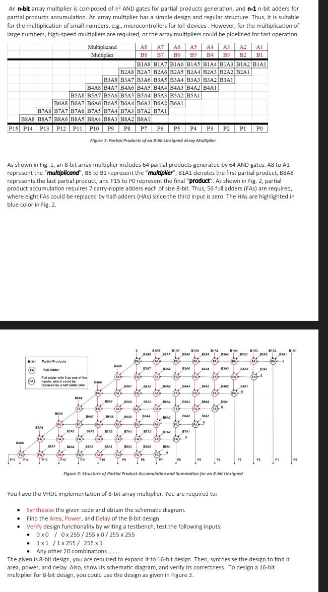
An n-bit array multiplier is composed of n2 AND gates for partial products generation, and n1n-bit adders for partial products accumulation. An array multiplier has a simple design and regular structure. Thus, it is suitable for the multiplication of small numbers, e.g., microcontrollers for loT devices. However, for the multiplication of large numbers, high-speed multipliers are required, or the array multipliers could be pipelined for fast operation. Figure 1: Partial Products of an 8-bit Unsigned Arroy Muitiplier As shown in Fig. 1, an 8 -bit array multiplier includes 64 partial products generated by 64 AND gates. A8 to A1 represent the "multiplicand", B8 to B1 represent the "multiplier", B1A1 denotes the first partial product, B8A8 represents the last partial product, and P15 to P0 represent the final "product". As shown in Fig. 2, partial product accumulation requires 7 carry-ripple adders each of size 8-bit. Thus, 56 full adders (FAs) are required, where eight FAs could be replaced by half-adders (HAs) since the third in put is zero. The HAs are highlighted in blue color in Fig. 2. Figure 2: Structure of Partal Mroduct Accumuronon and summation for an a-bit Unsigned You have the VHDL implementation of 8-bit array multiplier. You are required to: - Synthesise the given code and obtain the schematic diagram. - Find the Area, Power, and Delay of the 8-bit design. - Verify design functionality by writing a testbench, test the following inputs: - 00/0255/2550/255255 - 11/1255/2551 - Any other 20 combinations........ The given is 8-bit design, you are required to expand it to 16 -bit design. Then, synthesise the design to find it area, power, and delay. Also, show its schematic diagram, and verify its correctness. To design a 16-bit multiplier for 8-bit design, you could use the design as given in Figure 3Step by Step Solution
There are 3 Steps involved in it
Step: 1

Get Instant Access to Expert-Tailored Solutions
See step-by-step solutions with expert insights and AI powered tools for academic success
Step: 2

Step: 3
Ace Your Homework with AI
Get the answers you need in no time with our AI-driven, step-by-step assistance
Get Started
Financial and Managerial Accounting
Authors: Jonathan E. Duchac, James M. Reeve, Carl S. Warren
11th Edition
9780538480901, 9781111525774, 538480890, 538480904, 1111525773, 978-0538480895