

Question: A discrete common-source circuit with the configuration shown in Figure 4.17 is to be designed to provide a voltage gain of 18 and a symmetrical
A discrete common-source circuit with the configuration shown in Figure 4.17 is to be designed to provide a voltage gain of 18 and a symmetrical output voltage swing. The bias voltage is \(V_{D D}=3.3 \mathrm{~V}\), the output resistance of the signal source is \(500 \Omega\), and the transistor parameters are: \(V_{T N}=0.4 \mathrm{~V}\), \(k_{n}^{\prime}=100 \mu \mathrm{A} / \mathrm{V}^{2}\), and \(\lambda=0.01 \mathrm{~V}^{-1}\). Assume a quiescent drain current of \(I_{D Q}=100 \mu \mathrm{A}\).
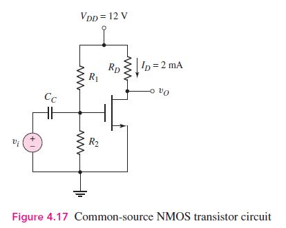
Vi 1+ Cc ww www VDD = 12 V R Rp R ID = 2 mA - vo Figure 4.17 Common-source NMOS transistor circuit
Step by Step Solution
3.47 Rating (160 Votes )
There are 3 Steps involved in it

Get step-by-step solutions from verified subject matter experts