The operation of a digital system is coordinated and controlled by a periodic waveform called a clock.
Question:
The operation of a digital system is coordinated and controlled by a periodic waveform called a clock. The clock waveform provides a standard timing reference to maintain synchronization between signal-processing results that become valid at different times during the clock cycle. Because of differences in digital circuit delays, there must be agreed-upon instants of time when circuit outputs can be treated as valid. The clock defers further signal processing until slower and faster outputs settle down when the clock signals the start of the next signal-processing cycle.
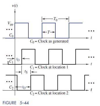
Figure 5–44 shows an idealized clock waveform as a periodic sequence of rectangular pulses. While we could easily write an exact expression for the clock waveform, we are interested here in discussing its partial descriptors. The first descriptor is the period T0 or equivalently the clock frequency f0 =1=T0. Clock frequency is a common measure of signal-processing speed and

can take values into the GHz range. The pulse duration T is the time interval in each cycle when the pulse amplitude is high (not zero). In waveform terminology the ratio of the time in the high state to the period, that is, T=T0, is called the duty cycle, usually expressed as a percentage. The pulse edges are the transition points at which the pulse changes states. There is a rising edge at the low-to-high transition and a falling edge at the high-to-low transition.
The pulse edges define the agreed-upon time instants at which the circuit outputs can be treated as valid inputs to other circuits. This means that circuit outputs must settle down during the time period between successive edges. Some synchronous operations are triggered by the rising edge and others by the falling edge. To provide equal settling times for both cases requiresequal time between edges. In other words, it is desirable for the clock duty cycle to be 50%. As a result, the clock waveform is essentially a raised square wave whose dc offset equals one half of the peak-to-peak value.
The system clock C0 in Figure 5–44 is generated at some point in a circuit and then distributed to other locations. The clock distribution network almost invariably introduces delays, as illustrated by C1 and C2 in Figure 5–44. Clock delay (tD) is defined as the time difference between a clock edge at a given location and the corresponding edge in the system clock at the point where it was generated. Delay is not necessarily a bad thing unless unequal delays cause the edges to be skewed, as indicated by the offset between C1 and C2 in Figure 5–44. When delays are significantly different, there is uncertainty as to instants of time at which further signal processing can safely proceed. This delay dispersion is called clock skew (tS), defined as the time difference between a clock edge at a given location and the corresponding edge at another location. Controlling clock skew is an important consideration in the design of the clock distribution network in high-speed very large-scale integrated (VLSI)
circuits.
Thus, partial descriptors of clock waveforms include frequency, duty cycle, edges, delay, and skew. The coming chapters treat dynamic circuits that modify input waveforms to produce outputs with different partial descriptors. In particular, dynamic circuit elements cause changes in a clock waveform, especially the partial descriptors of edges, delay, and skew.
Step by Step Answer:

The Analysis And Design Of Linear Circuits
ISBN: 9781119235385
8th Edition
Authors: Roland E. Thomas, Albert J. Rosa, Gregory J. Toussaint


