

Question: Calculate the small-signal model parameters g m , r o , C gs , and C gd for a NMOS transistor. Also calculate the gate-leakage
Calculate the small-signal model parameters gm, ro, Cgs, and Cgdfor a NMOS transistor. Also calculate the gate-leakage current IG. Assume the transistor operates in the active region with ID= 100 μA, VDS= 1V, VBS= 0 V, W = 0.5 m, and L = 0.1 μm. Use the transistor model data in Table 2.6.
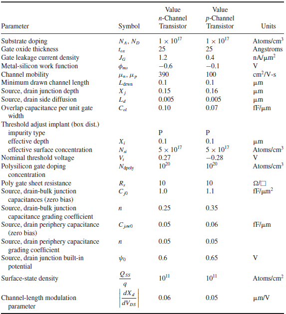
Value Value p-Channel Transistor n-Channel Parameter Symbol Transistor Units 1 x 10¹⁷ Atoms/cm Angstroms A/m? 1 107 NA, Np Substrate doping Gate oxide thickness 25 25 ter Gate leakage current density JG 1.2 0.4 Metal-silicon work function -0.6 -0.1 Channel mobility Minimum drawn channel length Source, drain junction depth Source, drain side diffusion Overlap capacitance per unit gate width cm?/V-s 390 0.1 100 0.1 Ldrwn um X; 0.15 0.16 um 0.005 0.005 La um 0.07 fF/m 0.10 Cel Threshold adjust implant (box dist.) impurity type effective depth 0.1 5 x 10¹⁷ -0.28 1020 X; 0.1 um Atoms/cm? 5 x 10¹⁷ effective surface concentration Ni V, Nominal threshold voltage Polysilicon gate doping 0.27 Atoms/cm 1020 Nagoly concentration Poly gate sheet resistance Source, drain-bulk junction capacitances (zero bias) Source, drain-bulk junction capacitance grading coefficient Source, drain periphery capacitance (zero bias) 10 1.1 10 R, fF/um? 1.0 0.35 0.25 0.05 0.06 fF/um Cjaw0 0.05 Source, drain periphery capacitance grading coefficient Source, drain junction built-in potential 0.05 0.65 0.6 Qss 10" Surface-state density 10" Atoms/cm2 dX a Channel-length modulation parameter 0.06 0.05 um/V dVps
Step by Step Solution
3.29 Rating (158 Votes )
There are 3 Steps involved in it
First estimate x d and L eff x d L eff and V ov V GS V t can be found ... View full answer

Get step-by-step solutions from verified subject matter experts
Document Format (2 attachments)
1528_605d88e1abb10_686803.pdf
180 KBs PDF File
1528_605d88e1abb10_686803.docx
120 KBs Word File