

Question: Problems in this exercise assume that the logic blocks used to implement a processors datapath have the following latencies: Register read is the time needed
Problems in this exercise assume that the logic blocks used to implement a processor’s datapath have the following latencies:
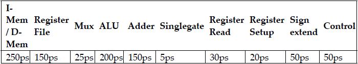
“Register read” is the time needed after the rising clock edge for the new register value to appear on the output. This value applies to the PC only. “Register setup” is the amount of time a register’s data input must be stable before the rising edge of the clock. This value applies to both the PC and Register File.
1. What is the latency of an R-type instruction (i.e., how long must the clock period be to ensure that this instruction works correctly)?
2. What is the latency of lw? (Check your answer carefully. Many students place extra muxes on the critical path.)
3. What is the latency of sw? (Check your answer carefully. Many students place extra muxes on the critical path.)
4. What is the latency of beq?
5. What is the latency of an arithmetic, logical, or shift
I-type (non-load) instruction?
6. What is the minimum clock period for this CPU?
I- Mem Register /D- File Mem 250ps 150ps 25ps 200ps 150ps 5ps Mux ALU Adder Singlegate Register Register Sign Read Setup extend Control 30ps 20ps 50ps 50ps
Step by Step Solution
3.42 Rating (161 Votes )
There are 3 Steps involved in it
Using the supplied logic block latencies lets address each question to find the lowest clock period ... View full answer

Get step-by-step solutions from verified subject matter experts