All Matches
Solution Library
Expert Answer
Textbooks
Search Textbook questions, tutors and Books
Oops, something went wrong!
Change your search query and then try again
Toggle navigation
FREE Trial
S
Books
FREE
Tutors
Study Help
Expert Questions
Accounting
General Management
Mathematics
Finance
Organizational Behaviour
Law
Physics
Operating System
Management Leadership
Sociology
Programming
Marketing
Database
Computer Network
Economics
Textbooks Solutions
Accounting
Managerial Accounting
Management Leadership
Cost Accounting
Statistics
Business Law
Corporate Finance
Finance
Economics
Auditing
Hire a Tutor
AI Study Help
New
Search
Search
Sign In
Register
study help
computer science
fundamentals digital logic
Questions and Answers of
Fundamentals Digital Logic
Discuss the basic differences between CISC and RISC.
Consider the following algorithm: Declare registers A [8], B [8], C [8];START:A ← 0; B ← 00001010;LOOP: A ← A + B; B ← B – 1;If B < > 0 then go to LOOP C ← A;HALT: Go to
What is the basic difference between main memory and secondary memory?
A microcontroller has 24 address pins. What is the maximum size of the main memory?
What is the basic difference between:(a) EPROM and EEPROM?(b) SRAM and DRAM?
Given a memory with a 14-bit address and an 8-bit word size. (a) How many bytes can be stored in this memory?(b) If this memory were constructed from 1K 1 RAMs, how many memory chips would
(a) How many address and data lines are required for a 1M 16 memory chip?(b) What is the size of a decoder with one chip enable (CE) to obtain a 64K 32 memory from 4K 8 chips? Where
A microcontroller with 24 address pins and eight data pins is connected to a 1K 8 memory with one enable. How many unused address bits of the microcontroller are available for interfacing other
Name the methods used in main memory array design. What are the advantages and disadvantages of each?
What is meant by foldback in linear decoding?
Define the three types of I/O. Identify each as either CPU-initiated or deviceinitiated.
What is the basic difference between standard I/O and memory-mapped I/O? Identify the programmed I/O technique used by the PIC18F.
What is the difference between memory mapping in a microcontroller and memory-mapped I/O?
Discuss the basic difference between polled I/O and interrupt I/O.
What is the difference between subroutine and interrupt I/O?
What is an interrupt address vector?
Summarize the basic difference between maskable and nonmaskable interrupts. Describe how power failure interrupt is normally handled.
Discuss the basic difference between internal and external interrupts.
What is the basic difference between a microprocessor, a single-chip microcomputer and a microcontroller?
What is meant by an 8-bit microcontroller? Name one commercially available 8-bit microcontroller.
What are the difference between(a) A program counter and a memory address register?(b) General-purpose register and instruction register?
How many bits are needed to access a 4 MB main memory? What is the hexadecimal value of the last address in this memory?
If the last address of an on-chip memory of a microcontroller is 0x7FF, determine its size.
What is the difference between von Neumann and Harvard CPU architectures? Provide an example of a commercially available microcontroller using each type of CPU.
What is the basic difference between program execution by a conventional CPU and the PIC18F CPU?
Discuss briefly the purpose of the functional units (CCP, ADC, serial communication) implemented in the PIC18F?
What is meant by pipelining?
Summarize the basic features of PIC18The PIC18F implements a two-stage pipeline. The PIC18F CPU fetches the instruction during the first stage. However, during the second stage, the PIC18F CPU while
What is the basic difference between assembly and high-level languages? Why would you choose one over the other?
Assume that two microcontrollers, the PIC18F and the HC16, have C compilers. Will a program written in C language run on both microcontrollers?
Will a program written in Microchip’s PIC18F assembly language run on microcontrollers from other manufacturers?
Write a C language statement to configure(a) All bits of Port C as inputs(b) All bits of Port D as outputs(c) Bits 0 through 4 of Port B as input(d) All bits of Port A as outputs
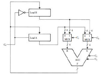
Consider the registers and ALU shown in Figure P6.22: The interpretation of various control points are summarized as follows:Answer the following questions by writing suitable control word(s). Each
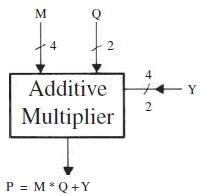
Design an unsigned 8 × 4 non-additive multiplier using additive-multiplier module whose block diagram representation is as follows: Assume that M, Q, and Y are unsigned integers. M 4 2 Additive
Design and implement a 6 × 6 array multiplier.
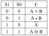
(a) Using a 4-bit binary adder with inputs (A, B, and Cin), outputs (F and Cout), and one selection bit (S0), design an arithmetic circuit as follows: S0 FUNCTION TO BE PERFORMED0
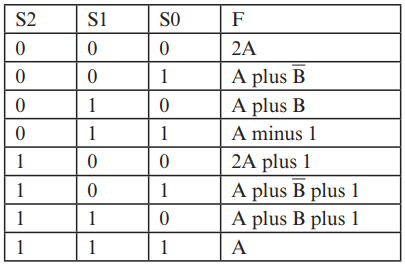
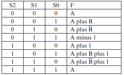
Design a 4-bit, 8-function arithmetic unit that will meet the following specifications: S2 0 0 0 0 1 1 1 1 S1 0 0 1 1 0 0 1 1 SO 0 1 0 1 0 1 0 1 F 2A A plus B A plus B A minus 1 2A plus 1 A plus B
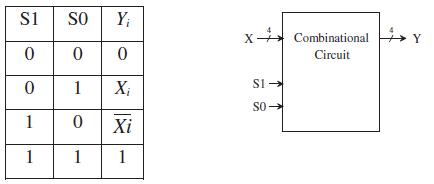
i) Design a combinational circuit that will work as follows: ii) Using the results of part i), design a 4-bit, 8-function arithmetic unit that will function as follows: S1 SO Y 0 0 0 0 1 X 1 0 1 1
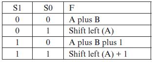
Design and implement a combinational circuit that will work as follows: Note that A and B are 4-bit operands. S1 0 0 1 1 SO 0 1 0 1 F A plus B Shift left (A) A plus B plus 1 Shift left (A) + 1
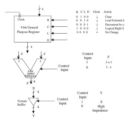
Repeat Problem 6.13 using microprogramming. Data From Problem 13Using the following components: 4-bit general-purpose register, 4-bit adder/ subtractor, and tristate buffer, and assuming the inbus
Using the following components: 4-bit general-purpose register, 4-bit adder/ subtractor, and tristate buffer, and assuming the inbus and outbus are 4 bits wide, design a control unit using hardwired
What is the basic difference between hardwired control, and microprogramming? Name the technique used for designing the control unit of the PIC18F and the HC11microcontrollers.
Discuss briefly the advantages and disadvantages of single-bus, two-bus, and three-bus architectures inside a control unit.
Draw a logic diagram to implement the following register transfers: (a) If the content of the 8-bit register R is odd, then x ← x ⊕ y, else x ← x AND yAssume x and y are 4 bits wide.(b) If
What is the purpose of the control unit in the CPU?
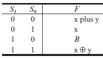
Design an ALU to perform the following operations:Assume that x and y are 4-bit numbers, and B = y̅3 y̅2 y̅1 y̅0. Draw a logic diagram. S, S, F x plus y 1 X 1 B 1
Design a 4-bit arithmetic unit as follows:Assume that A and B are 4-bit numbers. S 0 1 F A plus B A plus 1
Design a 4-bit ALU to perform the following operations: Assume that A is a 4-bit number. Draw a logic diagram using a binary adder, multiplexers, and inverters as necessary. S 0 1 F Logical Left
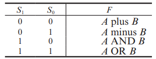
Design an arithmetic logic unit to perform the following functions: Use multiplexers, binary adders, and gates as needed. Assume that A and B are 4-bit numbers. Draw a logic circuit. S 0 0 1 1 So 0
Design: (a) A 16-bit adder whose worst-case add-time is 10Δ using a 4-bit CLA as a building block.(b) The fastest 64-bit adder using a 4-bit CLA as the building block. Estimate the worst-case
Using a 4-bit CLA as the building block, design an 8-bit adder.
Draw a logic diagram for a 4 4 barrel shifter.
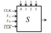
Design a combinational logic shifter with 4-bit input and 4-bit output as follows:where X means don’t care. Using multiplexers and tristate buffers, draw a logic diagram. Shift Count 4- bit output
Write a Verilog description using behavioral modeling for:(a) The positive edge-triggered JK Flip-Flop of Figure 5.9.(b) A D flip-flop with a synchronous reset input and a positive edge triggered
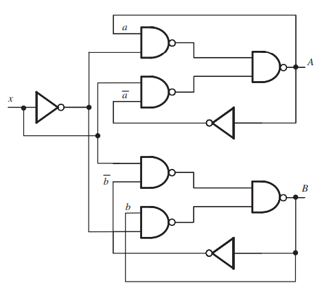
Derive the output equations for the asynchronous sequential circuit shown in Figure P5.34. Also, determine the state table and flow table. X a a Do Do Da Da Do Dop A B
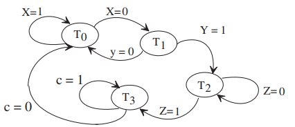
Draw an ASM chart for the following state diagram of Figure P5.33: Assume that the system stays in initial state T0 when control input c = 0 and input X = 1. The sequence of operations is started
Draw an ASM chart for each of the following sequence of operations:(a) The ASM chart will define a conditional operation to perform the operation R2← R2 – R1 during State T0 and will transfer
Draw an ASM chart for the following: Assume three states (a, b, c) in the system with one input x and two registers R1 and R2. The circuit is initially in state a. If x = 0, the control goes from
Given a memory with a 24-bit address and 8-bit word size,(a) How many bytes can be stored in this memory?(b) If this memory were constructed from 1K 1-bit RAM chips, how many memory chips would
What is the basic difference between SRAM and DRAM?
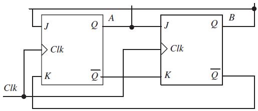
Assuming AB = 10, verify that the 2-bit counter shown in Figure P5.28 is a ring counter. Derive the state diagram. Clk Clk K Q Q A J Clk K Q Q B
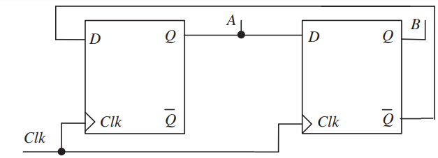
Consider the 2-bit Johnson counter shown in Figure P5.27. Derive the state diagram. Assume the D flip-flops are initialized to A = 0 and B = 0. Clk D Clk Q Q A D Clk Q Q B
Design a logic diagram that will generate 19 timing signals. Use a ring counter with JK flip-flops.
Use Figure P5.25 as the building block: Design a 4-bit general-purpose register as follows: S So Function 0 0 0 1 1 0 1 1 Load external data Rotate left; (AoA3, Ai-Ai-1 for i = 1,2,3) Rotate right;
Design the following nonbinary sequence counters using the type of flipflop specified. Assume the unused states as don’t cares. Is the counter self-correcting? Justify your answer. (a) Counting
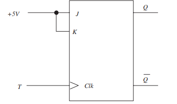
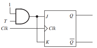
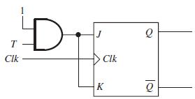
Analyze the circuit shown in Figure P5.22 and show that it is equivalent to a T flip-flop. T Clk D Clk K Q la
Analyze the circuit shown in Figure P5.22 and show that it is equivalent to a T flip-flop. Clk Clk
Design a synchronous sequential circuit with one input x and one output y. The input x is a serial message, and the system reads x one bit at a time. The output y is 1 whenever the binary pattern 000
Design a two-bit counter that will count in the following sequence: 00, 11, 10, 01, and repeat. Using T flip-flops: (a) Draw a state diagram.(b) Derive a state table.(c) Implement the circuit.
Design a synchronous sequential circuit using D flip-flops for the state diagram shown in Figure P5.19. T Cik D Clk K Q Q
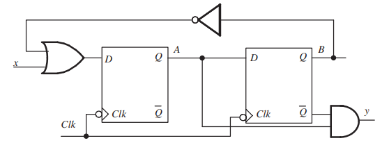
A sequential circuit contains two D flip-flops (A, B), one input (x), and one output (y), as shown in Figure P5.18. Derive the state table and the state diagram of the sequential circuit. Clk D Q Clk
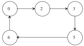
A synchronous sequential circuit is represented by the state diagram shown in Figure P5.17. Using JK flip-flops and undefined states as don’t cares: (a) Derive the state table.(b) Minimize the
A synchronous sequential circuit with two D flip-flops (a,b as outputs), one input (x), and an output (y) is expressed by the following equations: Da = ab̅x + a̅b, Db = x̅b + b̅xy = b̅x̅ +
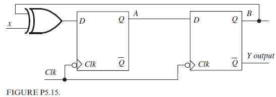
Analyze the clocked synchronous circuit shown in Figure P5.15. Express the next state in terms of the present state and inputs, derive the state table, and draw the state diagram. X A PITII D
Draw a logic circuit of the switch debouncer circuit using NAND gates.
Draw the block diagram of a T flip-flop using (a) JK ff (b) D ff
What are the advantages of a master–slave flip-flop?
What is the basic difference between an edge-triggered flip-flop and a latch?
Given the timing diagram for a negative-edge triggered T flip-flop in Figure P5.10, draw the timing diagram for Q. Assume Q is preset to 1 initially. CIk T FIGURE P5.10.
Given the timing diagram for a positive-edge-triggered D flip-flop in Figure P5.9, draw the timing diagrams for Q and Q̅. Assume Q is cleared to zero initially. CIk
Given Figure P5.8, draw the timing diagram for Q and Q̅ assuming a negative edge triggered JK flip-flop. Assume Q is preset to 1 initially. CIk K
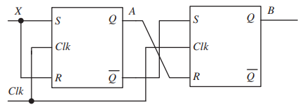
Assume that initially X = 0, A = 0, and B = 1 in Figure P5.7. Determine the values of A and B after one Clk pulse. Note that the latches are gated SR. |Clk Clk R Clk
Draw the logic diagram of a JK flip-flop using AND gates and inverters.
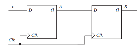
Assume that initially x = 1, A = 0, and B = 1 in Figure P5.5. Determine the values of A and B after the positive edge of Clk. A B х D D Clk Clk Clk
Draw the logic diagram of a D flip-flop using OR gates and inverters.
What is the basic difference between a latch and a flip-flop?
Identify the main characteristics of a synchronous sequential circuit and an asynchronous sequential circuit.
What is the basic difference between a combinational circuit and a sequential circuit?
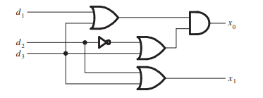
Write a Verilog description of the 4-to-2 priority encoder of Figure 4.16a(iii) using modeling of your choice. 'p d2 d3 х
Write a Verilog description for an 8-bit binary adder using hierarchical modeling.
Write a Verilog description for a 4-to-1 multiplexer using dataflow modeling using the conditional operator.
Write a Verilog description for a four-bit unsigned comparator using dataflow modeling using the “logical equality”, “less than”, and “greater than” operators.
Write a Verilog description for a 3-to-8 decoder with a LOW enable using:(a) Structural modeling(b) Behavioral modeling
Design a combinational circuit using a minimum number of full adders, and logic gates with one BCD to seven-segment converter (74LS47) and one common-anode seven-segment display, and which will
Design a 4-bit adder/subtractor (Example 4.7) using only full adders and EXCLUSIVE-OR gates. Do not use any multiplexers.
Design an 4K X 8 EPROM ( with two enable lines, CE and OE ) based system to display the squares of BCD digits on seven segment displays using a minimum number of 74LS47 BCD to seven segment
What is the technology used to fabricate EPROMs and EEPROMs?
What are the basic differences among PROM, PLA, PAL, PEEL and FPGA?
Design a combinational circuit using a 16 × 16 ROM that will increment a 4-bit unsigned number by 1. Determine the truth table and then draw a block diagram of your implementation showing the
Showing 1 - 100
of 180
1
2