

Question: The following register transfers are to be executed in the system of Fig. 5-4. For each transfer, specify: (1) The binary value that must be
The following register transfers are to be executed in the system of Fig. 5-4. For each transfer, specify:
(1) The binary value that must be applied to bus select inputs S2, S1, and S0;
(2) The register whose LD control input must be active (if any);
(3) A memory read or write operation (if needed); and
(4) The operation in the adder and logic circuit (if any).
a. AR←PC
b. IR←M[AR]
c. M[AR]←TR
d. AC←DR, DR←AC (done simultaneously)
Fig. 5-4
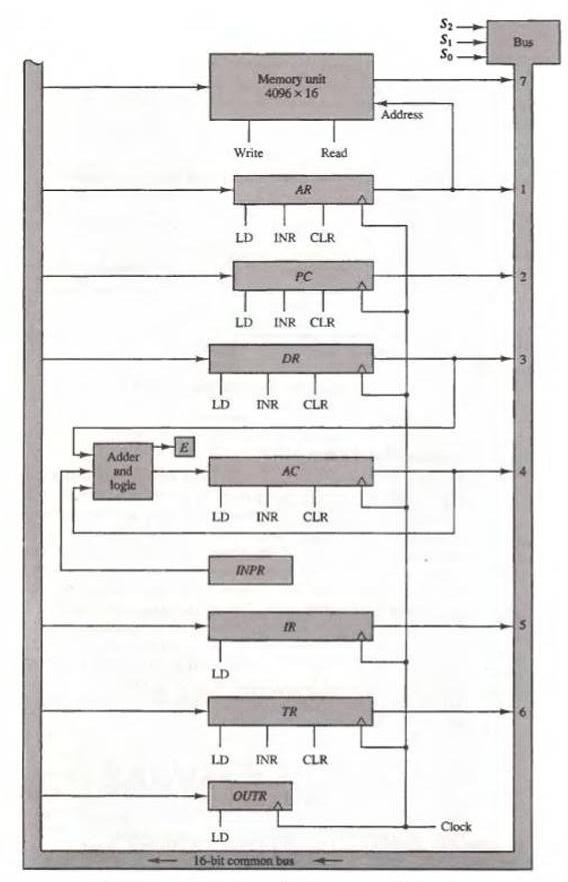
Adder and logic LD LD LD Write LD Memory unit 4096 x 16 LD LD INR INPR AR INR CLR OUTR INR INR CLR INR CLR PC DR AC Read IR TR LD 16-bit common bus CLR CLR Address Clock Bus 2
Step by Step Solution
3.48 Rating (171 Votes )
There are 3 Steps involved in it
The following register transfers are to be executed in the system of Fig 54 Here are the details for ... View full answer

Get step-by-step solutions from verified subject matter experts