Question
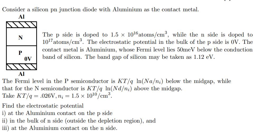
Consider a silicon pn junction diode with Aluminium as the contact metal. Al N P OV The p side is doped to 1.5 106

Consider a silicon pn junction diode with Aluminium as the contact metal. Al N P OV The p side is doped to 1.5 106 atoms/cm, while the n side is doped to 107 atoms/cm. The electrostatic potential in the bulk of the p side is OV. The contact metal is Aluminium, whose Fermi level lies 50meV below the conduction band of silicon. The band gap of silicon may be taken as 1.12 eV. Al The Fermi level in the P semiconductor is KT/q ln(Na/ni) below the midgap, while that for the N semiconductor is KT/q ln(Nd/ni) above the midgap. Take KT/q = .026V, n = 1.5 100/cm. Find the electrostatic potential i) at the Aluminium contact on the p side ii) in the bulk of n side (outside the depletion region), and iii) at the Aluminium contact on the n side.
Step by Step Solution
3.41 Rating (151 Votes )
There are 3 Steps involved in it
Step: 1
The detailed ...
Get Instant Access to Expert-Tailored Solutions
See step-by-step solutions with expert insights and AI powered tools for academic success
Step: 2

Step: 3

Ace Your Homework with AI
Get the answers you need in no time with our AI-driven, step-by-step assistance
Get StartedRecommended Textbook for
Understanding Basic Statistics
Authors: Charles Henry Brase, Corrinne Pellillo Brase
6th Edition
978-1133525097, 1133525091, 1111827028, 978-1133110316, 1133110312, 978-1111827021
Students also viewed these Electrical Engineering questions
Question
Answered: 1 week ago
Question
Answered: 1 week ago
Question
Answered: 1 week ago
Question
Answered: 1 week ago
Question
Answered: 1 week ago
Question
Answered: 1 week ago
Question
Answered: 1 week ago
Question
Answered: 1 week ago
Question
Answered: 1 week ago
Question
Answered: 1 week ago
Question
Answered: 1 week ago
Question
Answered: 1 week ago
Question
Answered: 1 week ago
Question
Answered: 1 week ago
Question
Answered: 1 week ago
Question
Answered: 1 week ago
Question
Answered: 1 week ago
Question
Answered: 1 week ago
Question
Answered: 1 week ago
Question
Answered: 1 week ago
Question
Answered: 1 week ago
View Answer in SolutionInn App


