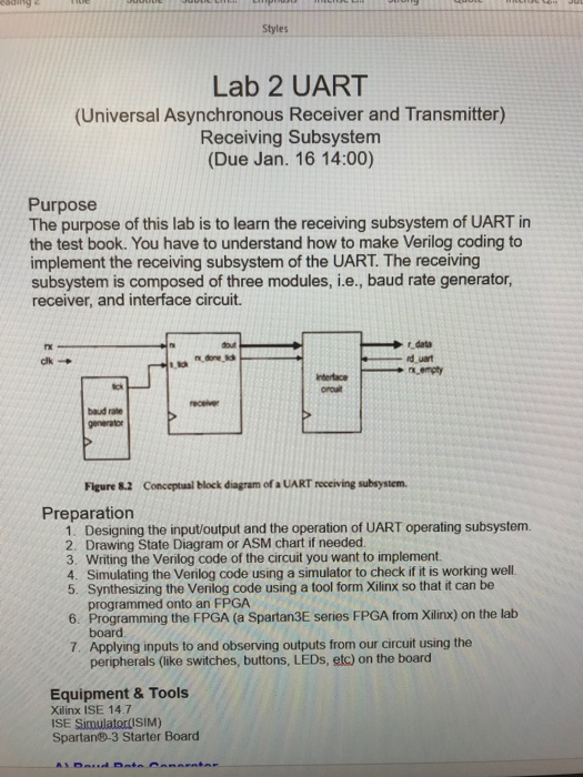
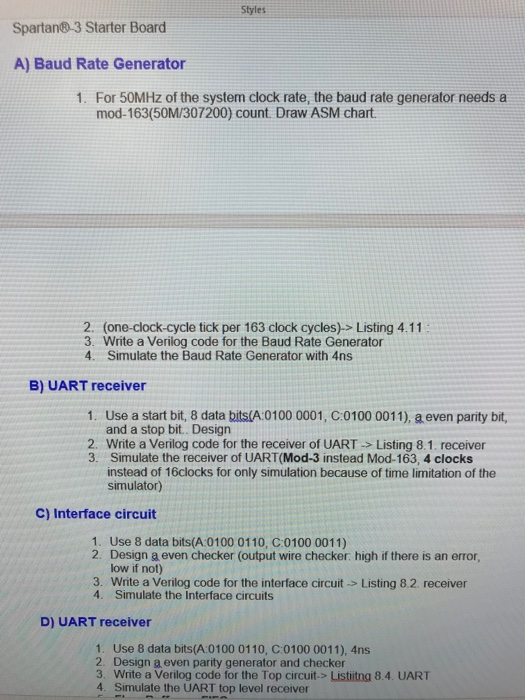
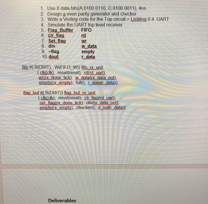
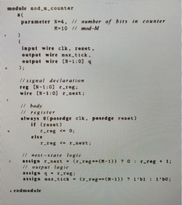
Lab 2 UART (Universal Asynchronous Receiver and Transmitter) Receiving Subsystem (Due Jan. 16 14:00) Purpose The purpose of this lab is to learn the receiving subsystem of UART in the test book. You have to understand how to make Verilog coding to implement the receiving subsystem of the UART. The receiving subsystem is composed of three modules, i.e., baud rate generator, receiver, and interface circuit. Figure 8.2 Conceptual block diagram of a UART receiving subsystem. Preparation 1. Designing the input/output and the operation of UART operating subsystem 2. Drawing State Diagram or ASM chart if needed 3. Writing the Verlog code of the circuit you want to implement. 4. Simulating the Venlog code using a simulator to check if it is working well 5. Synthesizing the Venlog code using a tool form Xilinx so that it can be programmed onto an FPGA 6. Programming the FPGA (a Spartan3E series FPGA from Xilinx) on the lab board 7. Applying inputs to and observing outputs from our circuit using the peripherals (like switches, buttons, LEDs, etc) on the board Equipment & Tools Xilinx ISE 14.7 ISE Simulator(SIM) Spartan-3 Starter Board Spartan-3 Starter Board A) Baud Rate Generator 1. For 50MHz of the system clock rate, the baud rate generator needs a mod-163(50M/307200) count. Draw ASM chart. 2. (one-clock-cycle tick per 163 clock cycles)-> Listing 4.11 3. Write a Verilog code for the Baud Rate Generator 4. Simulate the Baud Rate Generator with 4ns B) UART receiver 1. Use a start bit, 8 data bits(A:0100 0001, C:0100 0011), a even parity bit, and a stop bit.. Design 2. Write a Verilog code for the receiver of UART -> Listing 8.1. receiver 3. Simulate the receiver of UART(Mod-3 instead Mod-163, 4 clocks instead of 16clocks for only simulation because of time limitation of the simulator) C) Interface circuit 1. Use 8 data bits(A:0100 0110, C 0100 0011) 2. Design a even checker (output wire checker high if there is an error, low if not) 3. Write a Verilog code for the interface circuit Listing 8.2. receiver 4. Simulate the Interface circuits D) UART receiver 1. Use 8 data bits(A:0100 0110, C.0100 0011). 4ns 2. Design a even parity generator and checker 3. Write a Verilog code for the Top circuit-> Listiina 8.4. UART 4. Simulate the UART top level receiver 1. Use 8 data bits(A:0100 0110, C:0100 0011), 4ns 2. Design a even parity generator and checker 3. Write a Verilog code for the Top circuit-> Listiitng 8.4. UART 4. Simulate the UART top level receiver 5. Flag, Buffer FIFO 6. clc flag 7. Set flag wr 8. din w data 9. flag empty 10. dout data rd fifo #(.B(DBIT), W(FIFO_W)) fifo.cx unit (clkclk), reset(reset), dard uart), wrix done tick), w.data(rx data out), empty(xempty), full(). L.data(data)); flag.but #CB(DBIT)) flag buf.unit (clkcik), reset(reset), .cl flag(rd uart), set flagix done tick), din(x data out), empty.cx.empty), .checker(), d.out. data)); Deliverables module mod__counter parameter N-4, // number of bits in counter M-10 // mod-M input wire clk, reset. output wire max-tick, output wire [N-1:0) Il signal declaration reg (N-1:0) r_reg: wire [N-1:0) r.next: // body // register always (posedge clk, posedge reset) ir (reset) r_reg
