

Answered step by step
Verified Expert Solution
Question
1 Approved Answer
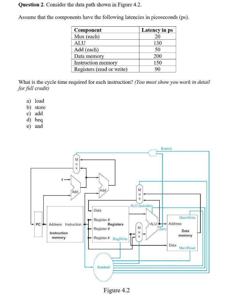
Question 2. Consider the data path shown in Figure 4.2. Assume that the components have the following latencies in picoseconds (ps). Component Mux (each) ALU
Step by Step Solution
There are 3 Steps involved in it
Step: 1

Get Instant Access to Expert-Tailored Solutions
See step-by-step solutions with expert insights and AI powered tools for academic success
Step: 2

Step: 3
Ace Your Homework with AI
Get the answers you need in no time with our AI-driven, step-by-step assistance
Get Started
Public Finance
Authors: Harvey Rosen, Ted Gayer
10th Global Edition
007715469X, 978-0077154691