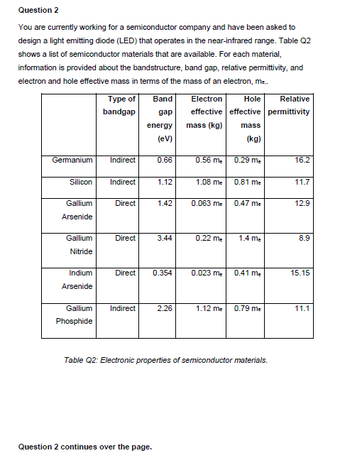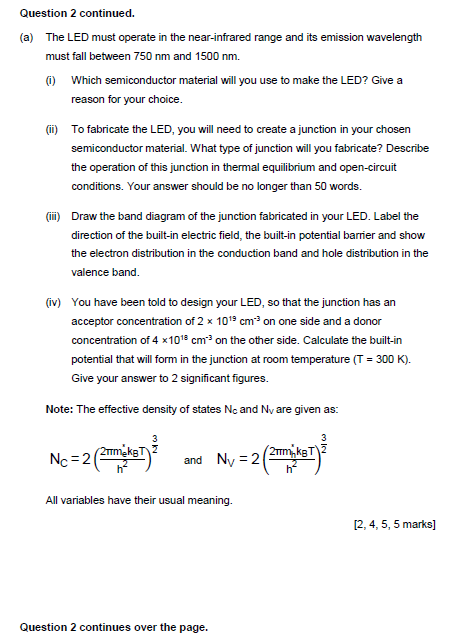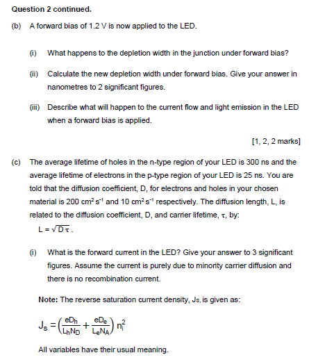


Question 2 You are currently working for a semiconductor company and have been asked to design a light emitting diode (LED) that operates in the near-infrared range. Table Q2 shows a list of semiconductor materials that are available. For each material, information is provided about the bandstructure, band gap, relative permittivity, and electron and hole effective mass in terms of the mass of an electron, me.. Type of Band Electron Hole Relative bandgap gap effective effective permittivity energy mass (kg) (eV) (kg) mass Germanium Indirect 0.66 0.56 me 0.29 me 16.2 Silicon Indirect 1.12 1.08 me 0.81 me 11.7 Direct 1.42 0.063 me 0.47 me 12.9 Gallium Arsenide Direct 3.44 0.22 me 1.4 me 8.9 Gallium Nitride Indium Direct 0.354 0.023 me 0.41 me 15.15 Arsenide Indirect 2.26 1.12 me 0.79 me 11.1 Gallium Phosphide Table Q2: Electronic properties of semiconductor materials. Question 2 continues over the page. Question 2 continued. (a) The LED must operate in the near-infrared range and its emission wavelength must fall between 750 nm and 1500 nm. 0 Which semiconductor material will you use to make the LED? Give a reason for your choice. () To fabricate the LED, you will need to create a junction in your chosen semiconductor material. What type of junction will you fabricate? Describe the operation of this junction in thermal equilibrium and open-circuit conditions. Your answer should be no longer than 50 words. (1) Draw the band diagram of the junction fabricated in your LED. Label the direction of the built-in electric field, the built-in potential barrier and show the electron distribution in the conduction band and hole distribution in the valence band. (iv) You have been told to design your LED, so that the junction has an acceptor concentration of 2 * 101 cm on one side and a donor concentration of 4 x 10 cm on the other side. Calculate the built-in potential that will form in the junction at room temperature (T = 300 K). Give your answer to 2 significant figures. Note: The effective density of states Nc and Ny are given as: um keT) Nc = 2 meket and Ny = 2 All variables have their usual meaning. [2, 4, 5, 5 marks] Question 2 continues over the page. Question 2 continued. (b) A forward bias of 1.2 V is now applied to the LED. What happens to the depletion width in the junction under forward bias? (i) Calculate the new depletion width under forward bias. Give your answer in nanometres to 2 significant figures. (I) Describe what will happen to the current flow and light emission in the LED when a forward bias is applied. [1, 2, 2 marks] (c) The average lifetime of holes in the n-type region of your LED is 300 ns and the average lifetime of electrons in the p-type region of your LED is 25 ns. You are told that the diffusion coefficient, D, for electrons and holes in your chosen material is 200 cm-s1 and 10 cm's" respectively. The diffusion length, L, is related to the diffusion coefficient, D, and carrier lifetime, t, by: LVDT. 0 What is the forward current in the LED? Give your answer to 3 significant figures. Assume the current is purely due to minority carrier diffusion and there is no recombination current. Note: The reverse saturation current density, Ja, is given as: eDh LAND eDe LENA All variables have their usual meaning. Question 2 You are currently working for a semiconductor company and have been asked to design a light emitting diode (LED) that operates in the near-infrared range. Table Q2 shows a list of semiconductor materials that are available. For each material, information is provided about the bandstructure, band gap, relative permittivity, and electron and hole effective mass in terms of the mass of an electron, me.. Type of Band Electron Hole Relative bandgap gap effective effective permittivity energy mass (kg) (eV) (kg) mass Germanium Indirect 0.66 0.56 me 0.29 me 16.2 Silicon Indirect 1.12 1.08 me 0.81 me 11.7 Direct 1.42 0.063 me 0.47 me 12.9 Gallium Arsenide Direct 3.44 0.22 me 1.4 me 8.9 Gallium Nitride Indium Direct 0.354 0.023 me 0.41 me 15.15 Arsenide Indirect 2.26 1.12 me 0.79 me 11.1 Gallium Phosphide Table Q2: Electronic properties of semiconductor materials. Question 2 continues over the page. Question 2 continued. (a) The LED must operate in the near-infrared range and its emission wavelength must fall between 750 nm and 1500 nm. 0 Which semiconductor material will you use to make the LED? Give a reason for your choice. () To fabricate the LED, you will need to create a junction in your chosen semiconductor material. What type of junction will you fabricate? Describe the operation of this junction in thermal equilibrium and open-circuit conditions. Your answer should be no longer than 50 words. (1) Draw the band diagram of the junction fabricated in your LED. Label the direction of the built-in electric field, the built-in potential barrier and show the electron distribution in the conduction band and hole distribution in the valence band. (iv) You have been told to design your LED, so that the junction has an acceptor concentration of 2 * 101 cm on one side and a donor concentration of 4 x 10 cm on the other side. Calculate the built-in potential that will form in the junction at room temperature (T = 300 K). Give your answer to 2 significant figures. Note: The effective density of states Nc and Ny are given as: um keT) Nc = 2 meket and Ny = 2 All variables have their usual meaning. [2, 4, 5, 5 marks] Question 2 continues over the page. Question 2 continued. (b) A forward bias of 1.2 V is now applied to the LED. What happens to the depletion width in the junction under forward bias? (i) Calculate the new depletion width under forward bias. Give your answer in nanometres to 2 significant figures. (I) Describe what will happen to the current flow and light emission in the LED when a forward bias is applied. [1, 2, 2 marks] (c) The average lifetime of holes in the n-type region of your LED is 300 ns and the average lifetime of electrons in the p-type region of your LED is 25 ns. You are told that the diffusion coefficient, D, for electrons and holes in your chosen material is 200 cm-s1 and 10 cm's" respectively. The diffusion length, L, is related to the diffusion coefficient, D, and carrier lifetime, t, by: LVDT. 0 What is the forward current in the LED? Give your answer to 3 significant figures. Assume the current is purely due to minority carrier diffusion and there is no recombination current. Note: The reverse saturation current density, Ja, is given as: eDh LAND eDe LENA All variables have their usual meaning
