Question
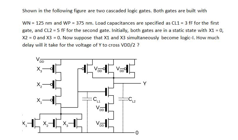
Shown in the following figure are two cascaded logic gates. Both gates are built with WN = 125 nm and WP = 375 nm.

Shown in the following figure are two cascaded logic gates. Both gates are built with WN = 125 nm and WP = 375 nm. Load capacitances are specified as CL1 = 3 ff for the first gate, and CL2= 5 ff for the second gate. Initially, both gates are in a static state with X1 = 0, X2 = 0 and X3 = 0. Now suppose that X1 and X3 simultaneously become logic-1. How much delay will it take for the voltage of Y to cross VDD/2 ? DD X X X- : DD DD VODO :CL2 0
Step by Step Solution
3.46 Rating (153 Votes )
There are 3 Steps involved in it
Step: 1
Answer Solution Explanation iThe gates ar...
Get Instant Access to Expert-Tailored Solutions
See step-by-step solutions with expert insights and AI powered tools for academic success
Step: 2

Step: 3

Ace Your Homework with AI
Get the answers you need in no time with our AI-driven, step-by-step assistance
Get StartedRecommended Textbook for
Income Tax Fundamentals 2013
Authors: Gerald E. Whittenburg, Martha Altus Buller, Steven L Gill
31st Edition
1111972516, 978-1285586618, 1285586611, 978-1285613109, 978-1111972516
Students also viewed these General Management questions
Question
Answered: 1 week ago
Question
Answered: 1 week ago
Question
Answered: 1 week ago
Question
Answered: 1 week ago
Question
Answered: 1 week ago
Question
Answered: 1 week ago
Question
Answered: 1 week ago
Question
Answered: 1 week ago
Question
Answered: 1 week ago
Question
Answered: 1 week ago
Question
Answered: 1 week ago
Question
Answered: 1 week ago
Question
Answered: 1 week ago
Question
Answered: 1 week ago
Question
Answered: 1 week ago
Question
Answered: 1 week ago
Question
Answered: 1 week ago
Question
Answered: 1 week ago
Question
Answered: 1 week ago
Question
Answered: 1 week ago
Question
Answered: 1 week ago
Question
Answered: 1 week ago
View Answer in SolutionInn App


