Where can I get these rough values from, appendix pages are below
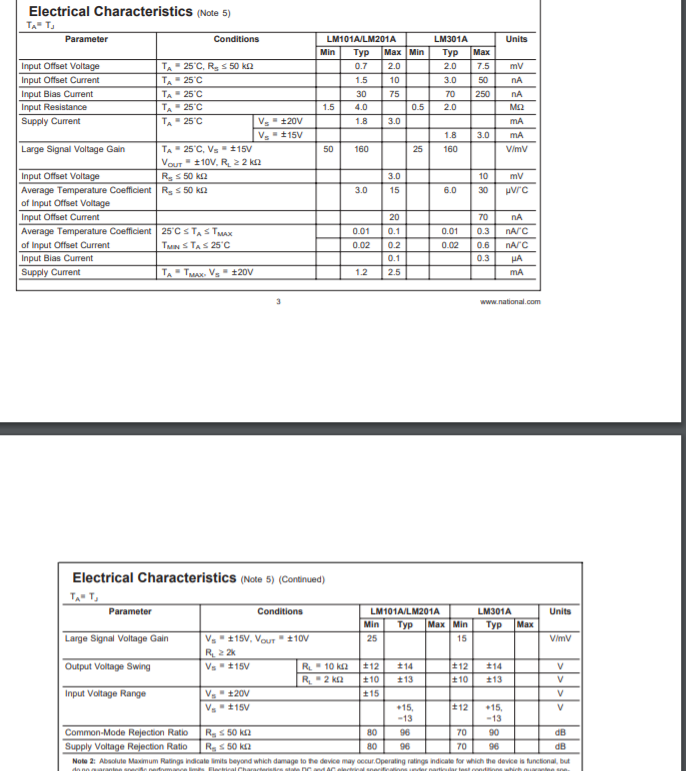
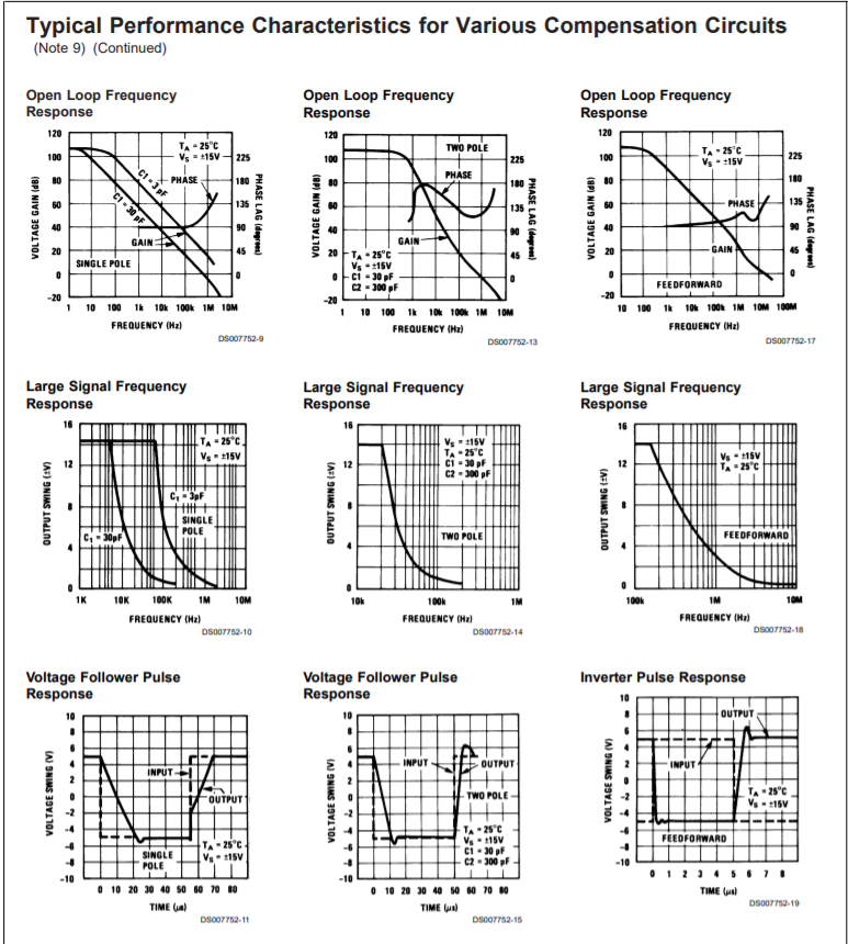
(a) From the information in the LM301 data sheets provided in appendix B (you can download from Moodle), estimate Ao, o and GBP for the LM301A. (b) Using PSpice simulation, verify the values of A, and GBP in 2(a). What happens to the frequency response by changing the Cc = 30pf to Cc = 3pf? Do the waveforms coincide with the Open Loop Frequency Response plot in the data sheet? (Refer to Pspice manual provided in Appendix F on how to set up the simulation) Electrical Characteristics (Note 5) TAT Parameter Conditions Units LM301A Typ 2.0 3.0 mV Input Offset Voltage Input Offset Current Input Bias Current Input Resistance Supply Current LM101A/LM201A Min Typ Max Min 0.7 2.0 1.5 10 30 75 1.5 4.0 0.5 1.8 3.0 TA -25C, RS s 50 k TA 25C TA - 25C TA 25C TA 25C Max 7.5 50 250 70 2.0 NA NA M2 mA MA VimV Vs20V Vs15V 3.0 1.8 160 50 160 25 Vout 3.0 15 10 30 mV uvrc 3.0 6.0 Large Signal Voltage Gain TA -25C, Vs -15V - 110V, R 2 2 Input Offset Voltage Rs 50 kn Average Temperature Coefficient Rs 50 k 2 of Input Offset Voltage Input Offset Current Average Temperature Coefficient CSTAS TMAX of Input Offset Current TMINSTAS 25C Input Bias Current Supply Current TA TMAX. V. 20V 20 0.01 0.02 0.1 0.2 0.1 0.01 0.02 70 0.3 0.6 0.3 NA NAC nA MA lolol 1.2 2.5 www.national.com Electrical Characteristics (Note 5) (Continued) 12 Parameter Conditions LM101A/LM201A LM301A Units Min Max Min Max Large Signal Voltage Gain Vs 15V. Vour 10V 25 15 VimV R 2 Output Voltage Swing Vs15V RL 10 kg 12 14 114 V R2 k +10 #13 10 13 v Input Voltage Range V200 15 V Vt15V 15 #12 15 V -13 Common-Mode Rejection Ratio R, 50 kn 80 96 70 90 dB Supply Voltage Rejection Ratio R 50 KR 80 96 70 96 dB Note 2: Absolute Masmum Ratings indicate limits beyond which damage to the device may occur Operating ratings indicate for which the device is functional, but -13 nnnnnn norm Electrical character Typical Performance Characteristics for Various Compensation Circuits (Note 9) (Continued) Open Loop Frequency Response Open Loop Frequency Response TWO POLE Open Loop Frequency Response 120 120 120 100 TA -25C Vs = +15V-225 100 225 100 TA -25C Vs +15V 225 PHASE 80 PHASE 180 180 80 180 C13pF 60 135 BO 135 PHASE 135 VOLTAGE GAIN (dB) C1-30 PHASE LAG degrees VOLTAGE GAIN (dB) PHASE LAG (deel! VOLTAGE GAIN (dB) PHASE LAG (de 40 90 90 GAIN 20 45 GAIN 40 GAIN 20 FTA -25C Vs +15V oci -30 pF C2 - 300 pF 45 SINGLE POLE -20 110 100 110k 100% IM 10M FREQUENCY (Hz) DSC07752-9 1 10 100 110k 100k 1M 10M FREQUENCY (H) DSC07752-13 FEEDFORWARD 10 100 110 100% 1M 10M 100M FREQUENCY (M21 DSC07752-17 Large Signal Frequency Response Large Signal Frequency Response Large Signal Frequency Response 16 16 Thu TA -25C Vs - 115V 12 Vs 15V TA -25C ci 30 pF C2-300 pF 12 Vs +15V TA -25C OUTPUT SWING (V) C, - 3pF tit SINGLE POLE OUTPUT SWING (V) OUTPUT SWING (V) C-30pF TWO POLE FEEDFORWARD 1K 10k IM 100 10K 100 M 10M FREQUENCY (NL) DSC07752.10 FREQUENCY CHI DSC07752-14 FREQUENCY (HE DSC07752.18 Voltage Follower Pulse Response Voltage Follower Pulse Response Inverter Pulse Response OUTPUT INPUT OUTPUT INPUT INPUT VOLTAGE SWING (V) VOLTAGE SWING (V) OUTPUT TA -25C TWO POLE VOLTAGE SWING (V) Vs +15V -"791 FEEDFORWARD TA -25C V-15V SINGLE POLE TA -25C V, 15V C1 - 30 pF C2 - 300 pF 7999 -10 0123 TIME 0 10 20 30 40 50 60 70 80 TIME DSC07752-11 0 10 20 30 40 50 60 70 80 TIME) DSC07752-15 DSC07752-19 (a) From the information in the LM301 data sheets provided in appendix B (you can download from Moodle), estimate Ao, o and GBP for the LM301A. (b) Using PSpice simulation, verify the values of A, and GBP in 2(a). What happens to the frequency response by changing the Cc = 30pf to Cc = 3pf? Do the waveforms coincide with the Open Loop Frequency Response plot in the data sheet? (Refer to Pspice manual provided in Appendix F on how to set up the simulation) Electrical Characteristics (Note 5) TAT Parameter Conditions Units LM301A Typ 2.0 3.0 mV Input Offset Voltage Input Offset Current Input Bias Current Input Resistance Supply Current LM101A/LM201A Min Typ Max Min 0.7 2.0 1.5 10 30 75 1.5 4.0 0.5 1.8 3.0 TA -25C, RS s 50 k TA 25C TA - 25C TA 25C TA 25C Max 7.5 50 250 70 2.0 NA NA M2 mA MA VimV Vs20V Vs15V 3.0 1.8 160 50 160 25 Vout 3.0 15 10 30 mV uvrc 3.0 6.0 Large Signal Voltage Gain TA -25C, Vs -15V - 110V, R 2 2 Input Offset Voltage Rs 50 kn Average Temperature Coefficient Rs 50 k 2 of Input Offset Voltage Input Offset Current Average Temperature Coefficient CSTAS TMAX of Input Offset Current TMINSTAS 25C Input Bias Current Supply Current TA TMAX. V. 20V 20 0.01 0.02 0.1 0.2 0.1 0.01 0.02 70 0.3 0.6 0.3 NA NAC nA MA lolol 1.2 2.5 www.national.com Electrical Characteristics (Note 5) (Continued) 12 Parameter Conditions LM101A/LM201A LM301A Units Min Max Min Max Large Signal Voltage Gain Vs 15V. Vour 10V 25 15 VimV R 2 Output Voltage Swing Vs15V RL 10 kg 12 14 114 V R2 k +10 #13 10 13 v Input Voltage Range V200 15 V Vt15V 15 #12 15 V -13 Common-Mode Rejection Ratio R, 50 kn 80 96 70 90 dB Supply Voltage Rejection Ratio R 50 KR 80 96 70 96 dB Note 2: Absolute Masmum Ratings indicate limits beyond which damage to the device may occur Operating ratings indicate for which the device is functional, but -13 nnnnnn norm Electrical character Typical Performance Characteristics for Various Compensation Circuits (Note 9) (Continued) Open Loop Frequency Response Open Loop Frequency Response TWO POLE Open Loop Frequency Response 120 120 120 100 TA -25C Vs = +15V-225 100 225 100 TA -25C Vs +15V 225 PHASE 80 PHASE 180 180 80 180 C13pF 60 135 BO 135 PHASE 135 VOLTAGE GAIN (dB) C1-30 PHASE LAG degrees VOLTAGE GAIN (dB) PHASE LAG (deel! VOLTAGE GAIN (dB) PHASE LAG (de 40 90 90 GAIN 20 45 GAIN 40 GAIN 20 FTA -25C Vs +15V oci -30 pF C2 - 300 pF 45 SINGLE POLE -20 110 100 110k 100% IM 10M FREQUENCY (Hz) DSC07752-9 1 10 100 110k 100k 1M 10M FREQUENCY (H) DSC07752-13 FEEDFORWARD 10 100 110 100% 1M 10M 100M FREQUENCY (M21 DSC07752-17 Large Signal Frequency Response Large Signal Frequency Response Large Signal Frequency Response 16 16 Thu TA -25C Vs - 115V 12 Vs 15V TA -25C ci 30 pF C2-300 pF 12 Vs +15V TA -25C OUTPUT SWING (V) C, - 3pF tit SINGLE POLE OUTPUT SWING (V) OUTPUT SWING (V) C-30pF TWO POLE FEEDFORWARD 1K 10k IM 100 10K 100 M 10M FREQUENCY (NL) DSC07752.10 FREQUENCY CHI DSC07752-14 FREQUENCY (HE DSC07752.18 Voltage Follower Pulse Response Voltage Follower Pulse Response Inverter Pulse Response OUTPUT INPUT OUTPUT INPUT INPUT VOLTAGE SWING (V) VOLTAGE SWING (V) OUTPUT TA -25C TWO POLE VOLTAGE SWING (V) Vs +15V -"791 FEEDFORWARD TA -25C V-15V SINGLE POLE TA -25C V, 15V C1 - 30 pF C2 - 300 pF 7999 -10 0123 TIME 0 10 20 30 40 50 60 70 80 TIME DSC07752-11 0 10 20 30 40 50 60 70 80 TIME) DSC07752-15 DSC07752-19