

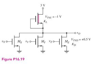
Consider a four-input NMOS NOR logic gate with a depletion load similar to the circuit in Figure
Question:
Consider a four-input NMOS NOR logic gate with a depletion load similar to the circuit in Figure P16.19. Assume \(V_{D D}=2.5 \mathrm{~V}, V_{T N D}=0.4 \mathrm{~V}\), and \(V_{T N L}=-0.6 \mathrm{~V}\). The maximum value of \(v_{O}\) in its low state is to be \(50 \mathrm{mV}\).
(a) Determine \(K_{D} / K_{L}\).
(b) The maximum power dissipation in this NOR logic gate is to be \(50 \mu \mathrm{W}\). Determine the width-to-length ratio of each transistor.
(c) Determine \(v_{O}\) when (i) two inputs are a logic 1, (ii) three inputs are a logic 1 , and (iii) all inputs are a logic 1 .
Fantastic news! We've Found the answer you've been seeking!
Step by Step Answer:

Answered By
Aysha Ali
my name is ayesha ali. i have done my matriculation in science topics with a+ . then i got admission in the field of computer science and technology in punjab college, lahore. i have passed my final examination of college with a+ also. after that, i got admission in the biggest university of pakistan which is university of the punjab. i am studying business and information technology in my university. i always stand first in my class. i am very brilliant client. my experts always appreciate my work. my projects are very popular in my university because i always complete my work with extreme devotion. i have a great knowledge about all major science topics. science topics always remain my favorite topics. i am also a home expert. i teach many clients at my home ranging from pre-school level to university level. my clients always show excellent result. i am expert in writing essays, reports, speeches, researches and all type of projects. i also have a vast knowledge about business, marketing, cost accounting and finance. i am also expert in making presentations on powerpoint and microsoft word. if you need any sort of help in any topic, please dont hesitate to consult with me. i will provide you the best work at a very reasonable price. i am quality oriented and i have 5 year experience in the following field.
matriculation in science topics; inter in computer science; bachelors in business and information technology
_embed src=http://www.clocklink.com/clocks/0018-orange.swf?timezone=usa_albany& width=200 height=200 wmode=transparent type=application/x-shockwave-flash_
11+ Reviews
14+ Question Solved
Related Book For 

Microelectronics Circuit Analysis And Design
ISBN: 9780071289474
4th Edition
Authors: Donald A. Neamen
Question Posted:
