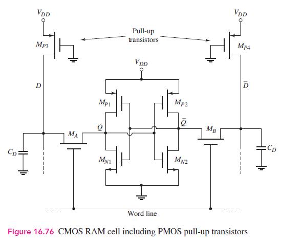
Consider the CMOS RAM cell and data lines in Figure 16.76 biased at (V_{D D}=2.5 mathrm{~V}). Assume
Question:
Consider the CMOS RAM cell and data lines in Figure 16.76 biased at \(V_{D D}=2.5 \mathrm{~V}\). Assume transistor parameters \(k_{n}^{\prime}=80 \mu \mathrm{A} / \mathrm{V}^{2}, k_{p}^{\prime}=35 \mu \mathrm{A} / \mathrm{V}^{2}\), \(V_{T N}=0.4 \mathrm{~V}, V_{T P}=-0.4 \mathrm{~V}, W / L=2\left(M_{N 1}\right.\) and \(\left.M_{N 2}\right), W / L=4\left(M_{P 1}\right.\) and \(M_{P 2}\) ), and \(W / L=1\) (all other transistors). If \(Q=0\) and \(\bar{Q}=1\), determine the steady-state values of \(D\) and \(\bar{D}\) after the row has been selected. Neglect the body effect.

Fantastic news! We've Found the answer you've been seeking!
Step by Step Answer:
Related Book For 

Microelectronics Circuit Analysis And Design
ISBN: 9780071289474
4th Edition
Authors: Donald A. Neamen
Question Posted:


