

Consider the NMOS inverter with depletion load in Figure 16.7(a). Let (V_{D D}=1.8 mathrm{~V}), and assume (V_{T
Question:
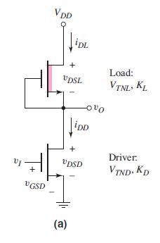
Consider the NMOS inverter with depletion load in Figure 16.7(a). Let \(V_{D D}=1.8 \mathrm{~V}\), and assume \(V_{T N D}=0.3 \mathrm{~V}\) and \(V_{T N L}=-0.6 \mathrm{~V}\).
(a) Design the circuit such that the power dissipation is \(80 \mu \mathrm{W}\) and the output voltage is \(v_{O}=0.06 \mathrm{~V}\) when \(v_{I}\) is a logic 1 .
(b) Using the results of part (a), determine the transition points for the driver and load transistors.
(c) If \((W / L)_{D}\) found in part (a) is doubled, what is the maximum power dissipation in the inverter and what is \(v_{O}\) when \(v_{I}\) is a logic 1 ?
Figure 16.7(a):-
Fantastic news! We've Found the answer you've been seeking!
Step by Step Answer:

Answered By
OTIENO OBADO
I have a vast experience in teaching, mentoring and tutoring. I handle student concerns diligently and my academic background is undeniably aesthetic
3+ Reviews
10+ Question Solved
Related Book For 

Microelectronics Circuit Analysis And Design
ISBN: 9780071289474
4th Edition
Authors: Donald A. Neamen
Question Posted:
