

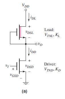
In the depletion-load NMOS inverter circuit in Figure 16.7(a), let (V_{T N D}=0.5 mathrm{~V}) and (V_{D D}=3
Question:
In the depletion-load NMOS inverter circuit in Figure 16.7(a), let \(V_{T N D}=0.5 \mathrm{~V}\) and \(V_{D D}=3 \mathrm{~V}, K_{L}=50 \mu \mathrm{A} / \mathrm{V}^{2}\), and \(K_{D}=500 \mu \mathrm{A} / \mathrm{V}^{2}\). Calculate the value of \(V_{T N L}\) such that \(v_{O}=0.10 \mathrm{~V}\) when \(v_{I}=3 \mathrm{~V}\).
Figure 16.7(a):-
Fantastic news! We've Found the answer you've been seeking!
Step by Step Answer:

Answered By
Utsab mitra
I have the expertise to deliver these subjects to college and higher-level students. The services would involve only solving assignments, homework help, and others.
I have experience in delivering these subjects for the last 6 years on a freelancing basis in different companies around the globe. I am CMA certified and CGMA UK. I have professional experience of 18 years in the industry involved in the manufacturing company and IT implementation experience of over 12 years.
I have delivered this help to students effortlessly, which is essential to give the students a good grade in their studies.
2+ Reviews
10+ Question Solved
Related Book For 

Microelectronics Circuit Analysis And Design
ISBN: 9780071289474
4th Edition
Authors: Donald A. Neamen
Question Posted:
