

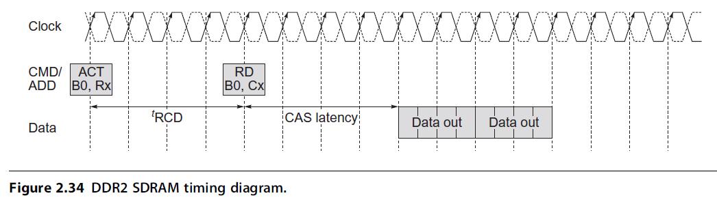
Question: A sample DDR2 SDRAMtiming diagram is shown in Figure 2.34. tRCD is the time required to activate a row in a bank, and column address
A sample DDR2 SDRAMtiming diagram is shown in Figure 2.34. tRCD is the time required to activate a row in a bank, and column address strobe (CAS) latency (CL) is the number of cycles required to read out a column in a row. Assume that the RAM is on a standard DDR2 DIMM with ECC, having 72 data lines. Also assume burst lengths of 8 that read out 8 bits, or a total of 64 B from the DIMM. Assume tRCD = CAS (or CL) clock_frequency, and clock_frequency = transfers_per_second/2. The on-chip latency
on a cache miss through levels 1 and 2 and back, not including the DRAM access, is 20 ns.
a. How much time is required from presentation of the activate command until the last requested bit of data from the DRAM transitions from valid to invalid for the DDR2-667 1 Gb CL¼5 DIMM? Assume that for every request, we automatically prefetch another adjacent cache line in the same page.
b. What is the relative latency when using the DDR2-667 DIMM of a read requiring a bank activate versus one to an already open page, including the time required to process the miss inside the processor?
Clock xxxxxxxxx CMD/ ACT ADD BO, Rx Data RCD RD BO, CX CAS latency Figure 2.34 DDR2 SDRAM timing diagram. Data out Data out
Step by Step Solution
There are 3 Steps involved in it
a This is similar to the scenario given in the fig... View full answer

Get step-by-step solutions from verified subject matter experts