

Question: A silicon p n junction diode is characterized by a junction capacitance C j defined as C j = K 0 A W where K
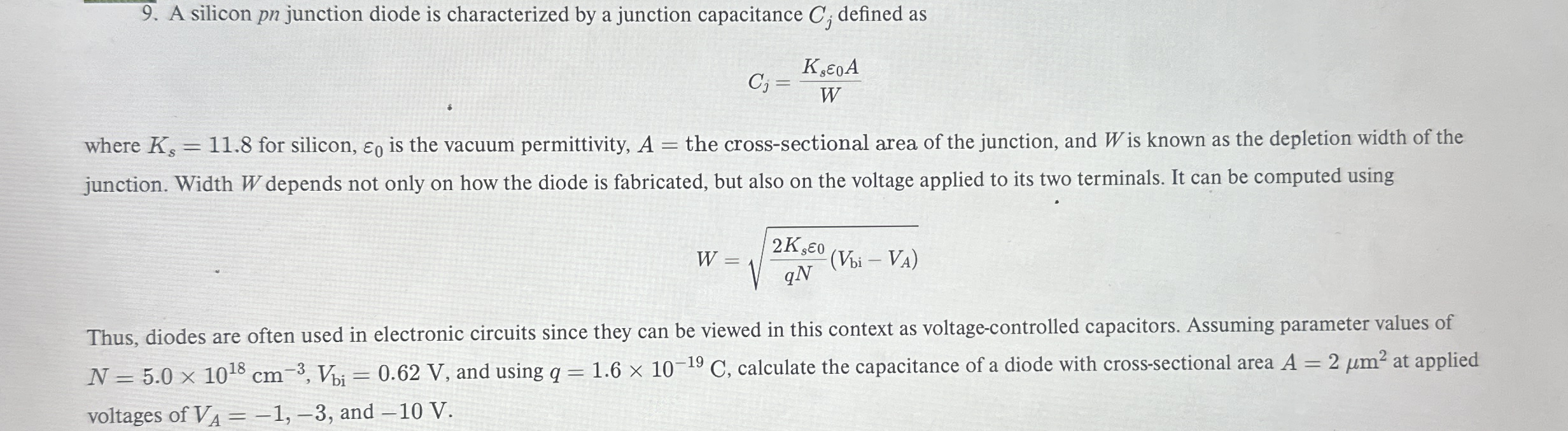
A silicon junction diode is characterized by a junction capacitance defined as
where for silicon, is the vacuum permittivity, the crosssectional area of the junction, and is known as the depletion width of the junction. Width depends not only on how the diode is fabricated, but also on the voltage applied to its two terminals. It can be computed using
Thus, diodes are often used in electronic circuits since they can be viewed in this context as voltagecontrolled capacitors. Assuming parameter values of and using calculate the capacitance of a diode with crosssectional area at applied voltages of and V
Step by Step Solution
There are 3 Steps involved in it
1 Expert Approved Answer
Step: 1 Unlock

Question Has Been Solved by an Expert!
Get step-by-step solutions from verified subject matter experts
Step: 2 Unlock
Step: 3 Unlock