

Question: Figure P9.23 shows a circuit for a differential amplifier with an active load. Here Q1 and Q2 form the differential pair, while the current
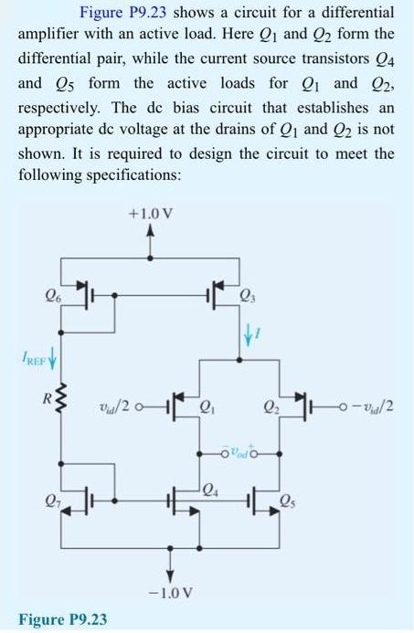
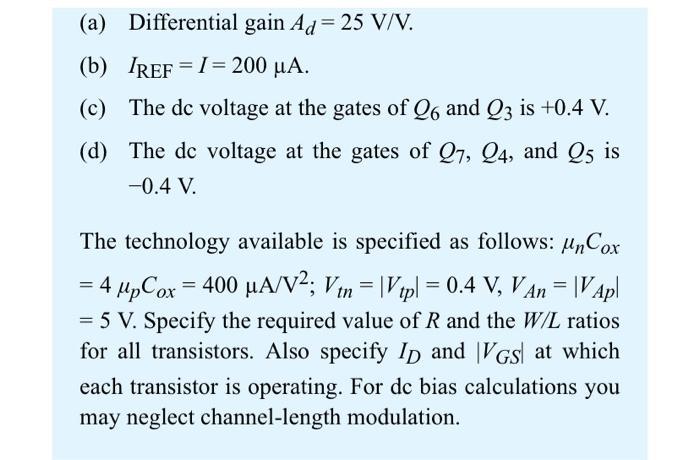
Figure P9.23 shows a circuit for a differential amplifier with an active load. Here Q1 and Q2 form the differential pair, while the current source transistors Q4 and Qs form the active loads for Q1 and Q2, respectively. The de bias circuit that establishes an appropriate de voltage at the drains of Q1 and Q2 is not shown. It is required to design the circuit to meet the following specifications: +1.0 V R Q2 Qs -1.0 V Figure P9.23 (a) Differential gain Ad = 25 V/V. (b) IREF = I= 200 A. (c) The de voltage at the gates of Q6 and Q3 is +0.4 V. (d) The de voltage at the gates of Q7, Q4, and Q5 is -0.4 V. The technology available is specified as follows: HnCox = 4 MpCox = 400 A/V; Vin = |Vipl = 0.4 V, VAn = |VApl = 5 V. Specify the required value of R and the W/L ratios for all transistors. Also specify Ip and |VGS at which each transistor is operating. For dc bias calculations you may neglect channel-length modulation.
Step by Step Solution
3.40 Rating (159 Votes )
There are 3 Steps involved in it
To design the differential amplifier in Figure P923 to meet the given specifications we need to determine the following Value of R WL ratios for all t... View full answer

Get step-by-step solutions from verified subject matter experts