

Question: T- en clock J C cir M EE598 Verilog Design Q Q' INPUT INBUT Q Q' TFF PRN T T Graphic symbol CLBN Q
![clock 89899 cir en Q1 02 Ops 25 ns clk enable reset inst 5.12 us count_out[2..0] Figure 4 C 10.24 us Figure 3](https://dsd5zvtm8ll6.cloudfront.net/si.experts.images/answers/2023/10/651dae0f7abf6_918651dae0eebc0c.jpg)
![InClass Exercise 2 cik enable reset clk three_bit_counter Ops 5 ns count_out[2] count_out[1] count_out[0] clk](https://dsd5zvtm8ll6.cloudfront.net/si.experts.images/answers/2023/10/651dae10a5079_920651dae10055da.jpg)
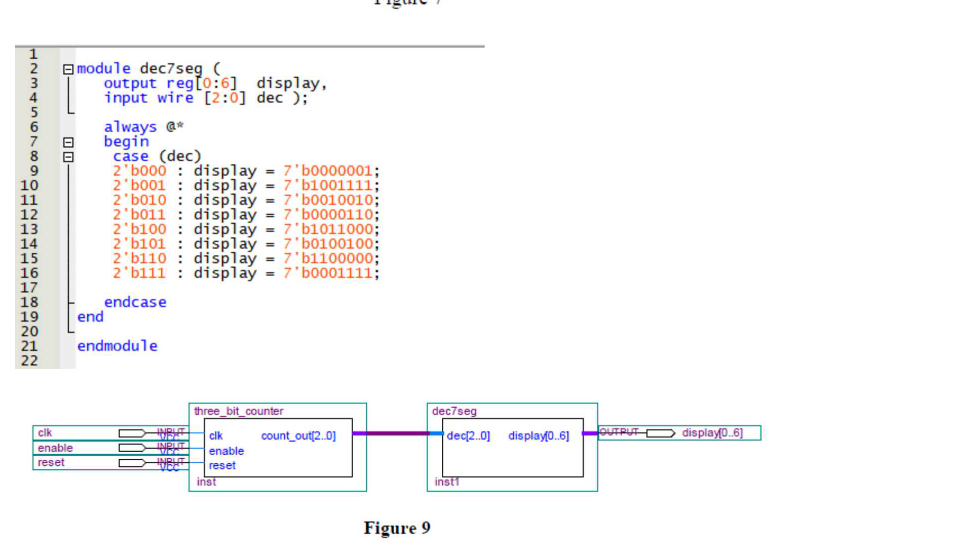
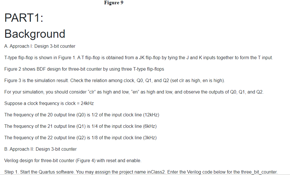
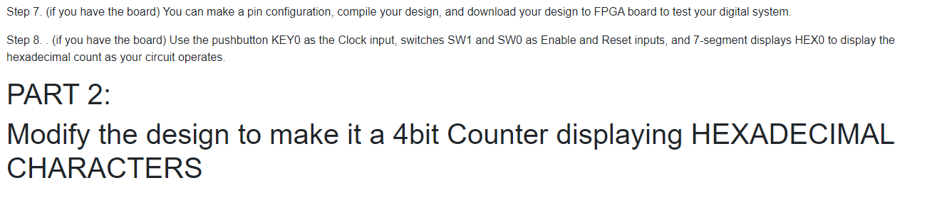
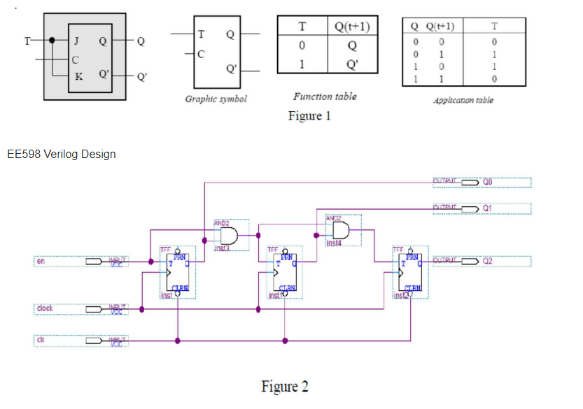
T- en clock J C cir M EE598 Verilog Design Q Q' "INPUT INBUT Q Q' TFF PRN T T Graphic symbol CLBN Q AND2 TFF T CLBN inst T 0 1 Function table Figure 1 Q(t+1) Q Q' Figure 2 JANDZ ins14 STEF Q Q(+1) 0 1 0 1 0 0 1 1 LEN PROMBOY Application table OUTPUT k T 0 1 OUTPUT 0 Q1 Q2 clock 89899 cir en Q1 02 Ops 25 ns clk enable reset inst 5.12 us count_out[2..0] Figure 4 C 10.24 us Figure 3 15.36 us 20.0 us InClass Exercise 2 cik enable reset clk three_bit_counter Ops 5 ns count_out[2] count_out[1] count_out[0] clk enable reset inst Figure 6 Designing a Multi-bit Counter and Programming on DE10-Lite count_out[2..0] 5.12 us 10.24 us reset enable count_out @[11X121 (13) (41) (51) (161) (71X10X12X OUTPUT 15.36 us count_out[2..01 Figure 7 20.48 us 101 25. us 30.0 us LLLLAAAANNN 890000 VOSTWNTOCOLOSAWNT 2 3 9 10 11 12 13 14 15 16 17 18 19 20 00 22 module dec7seg ( cik enable reset output reg[0:6] display, input wire [2:0] dec );" always @* begin case (dec) end 2'b000 2 b001 2 b010 2 b011 2 b100 2'b101 2 b110 2'b111: 21 endmodule endcase INPUT MWEZ INPUT Wala INPUT WEE = display 7'b0000001; display = 7'b1001111; display = 7'b0010010; display = 7'b0000110; display = 7'b1011000; display = 7'b0100100; display = 7'b1100000; display = 7'b0001111; three_bit_counter clk enable reset inst count_out[2..0] Figure 9 dec7seg dec[2..0] display[0..6] insti OUTPUT display(0..6] Figure 9 PART 1: Background A. Approach I: Design 3-bit counter T-type flip-flop is shown in Figure 1. A T flip-flop is obtained from a JK flip-flop by tying the J and K inputs together to form the T input. Figure 2 shows BDF design for three-bit counter by using three T-type flip-flops Figure 3 is the simulation result. Check the relation among clock, QO, Q1, and Q2 (set clr as high, en is high). For your simulation, you should consider "clr" as high and low, "en" as high and low, and observe the outputs of Q0, Q1, and Q2. Suppose a clock frequency is clock = 24kHz The frequency of the 20 output line (Q0) is 1/2 of the input clock line (12kHz) The frequency of the 21 output line (Q1) is 1/4 of the input clock line (6kHz) The frequency of the 22 output line (Q2) is 1/8 of the input clock line (3kHz) B. Approach II: Design 3-bit counter Verilog design for three-bit counter (Figure 4) with reset and enable. Step 1. Start the Quartus software. You may asssign the project name inClass2. Enter the Verilog code below for the three_bit_counter. Step 3. Save the Verilog file (Figure 5) as three_bit_counter.v as part of our project under your subfolder. Place a check mark in the space labeled Add file to current project and press Save Step 4. Select File - Create/Update - Create Symbol Files for Current File (three_bit_counter.bsf symbol) to create a symbol file for the Verilog code entered. A Compilation Report window initially displays "Report not available"; however, be patient. A display window should soon appear stating that the Create Symbol File was (or not) successful. Click OK and close the Compilation Report window. Step 5. Open a new Schematic file (File > New) by highlighting Block Diagram/Schematic File. And click OK. Find the symbol file (bsf file you just created for Verilog in Step 4) from Project folder to support your design in BDF view. Insert the symbol and input/output pins. Note that multi-bit buses "Properties" must be used to rename the port signal as [MSB..LSB]. In our case, count_out[2..0] will be the correct format. Step 6. Before compiling this bdf file, we need to name this bdf file and save it as part of our project under your subfolder. Choose File > Save As and enter File name as counter3. Place a check mark in the space labeled Add file to current project and press Save. Step 7. create a Vector Waveform File (vwf) to simulate a design(bdf) file. Set an end time 30 s for simulation from Edit and then run simulation based on Figure 3. You may have to expand the size of the Simulation Waveforms to suit your need and choose View > Fit in Window to see the entire 30s waveform. Figure 7 is the simulation result. Check the relation among clock, reset, enable, count_out[0], count_out[1], count_out[2]. Integrate the decoder with 3-bit counter Step 1. design a decoder in Verilog (Figure 8) Step 2. Save the Verilog file as dec7seg v as part of our project under your subfolder. Place a check mark in the space labeled Add file to current project and press Save Step 3. Select File - Create/Update - Create Symbol Files for Current File (dec7seg.bsf symbol) to create a symbol file for the Verilog code entered. Step 4. Open a new Schematic file (File > New) by highlighting Block Diagram/Schematic File. And click OK. Find the symbol file (bsf file you created for Verilog) from Project folder to support your design in BDF view. Insert the symbol and input/output pins Step 7. (if you have the board) You can make a pin configuration, compile your design, and download your design to FPGA board to test your digital system. Step 8.. (if you have the board) Use the pushbutton KEYO as the Clock input, switches SW1 and SWO as Enable and Reset inputs, and 7-segment displays HEXO to display the hexadecimal count as your circuit operates. PART 2: Modify the design to make it a 4bit Counter displaying HEXADECIMAL CHARACTERS
Step by Step Solution
3.33 Rating (144 Votes )
There are 3 Steps involved in it
It appears youve shared images of a digital design exercise focusing on building a multibit counter using flipflops and programming the design on an F... View full answer

Get step-by-step solutions from verified subject matter experts