New Semester
Started
Get
50% OFF
Study Help!
--h --m --s
Claim Now
Question Answers
Textbooks
Find textbooks, questions and answers
Oops, something went wrong!
Change your search query and then try again
S
Books
FREE
Study Help
Expert Questions
Accounting
General Management
Mathematics
Finance
Organizational Behaviour
Law
Physics
Operating System
Management Leadership
Sociology
Programming
Marketing
Database
Computer Network
Economics
Textbooks Solutions
Accounting
Managerial Accounting
Management Leadership
Cost Accounting
Statistics
Business Law
Corporate Finance
Finance
Economics
Auditing
Tutors
Online Tutors
Find a Tutor
Hire a Tutor
Become a Tutor
AI Tutor
AI Study Planner
NEW
Sell Books
Search
Search
Sign In
Register
study help
computer science
computer architecture
Computer Organization And Architecture Themes And Variations 1st Edition Alan Clements - Solutions
From first principles, derive an expression for the speedup ratio of a memory system with cache ( assume the hit ratio is h and the ratio of the main storage access time to cache access time is k, where k < 1). Assume that the system is an ideal system and that you don't have to worry about the
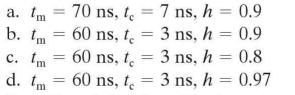
For the following ideal systems, calculate the speedup ratio S. In each case , te is the access time of the cache memory, tm is the access time of the main store, and h is the hit ratio. 70 ns, t = 7 ns, h= 0.9 60 ns, t = 3 ns, h = 0.9 = 3 ns, h= 0.8 c. tm = 60 ns, te 60 ns, t d. tm 60 ns, t = 3
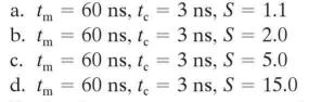
For the following ideal systems, calculate the hit ratio h required to achieve the stated speedup ratio S. a. tm b. Im c. tm d. m 60 ns, t 60 ns, t = 3 ns, S = 1.1 = 3 ns, S = 2.0 60 ns, t = 3 ns, S = 5.0 60 ns, te= 3 ns, S = 15.0
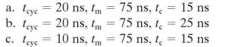
Real microprocessors operate in time slots of a given duration (i.e. , an integer multiple of the clock period). For example, if the clock has a speed of 100 MHz, the clock cycle time is 10 ns, and all operations must take an integer number of 10 ns units. The following data gives the clock cycle
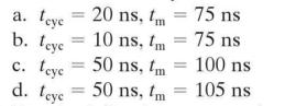
For the following systems that use a clocked microprocessor, calculate the maximum speedup ratio you could expect to see ash approaches 100%. a. teye b. Leye c. teye 20 ns, tm 20 ns, m Im = 75 ns, te 75 ns, t = 10 ns, tm75 = 75 ns, te ns, t, = 15 ns 25 ns 15 ns
In practice, a computer spends a fraction of the time performing internal operations as well as memory accesses. Consequently, the effective speedup ratio is reduced, because cache memory has no effect on internal operations. The average time required to execute an instruction can be written as.
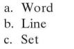
In a direct-mapped cache memory system, what 1s the meaning of the following terms. a. Word b. Line c. Set
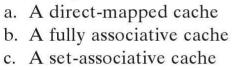
How is data in main store mapped on to each of the following? a. A direct-mapped cache b. A fully associative cache c. A set-associative cache
Why is it so difficult to construct an associative cache?
Why is the set-associative cache so popular?
With the aid of a diagram, show how a cache-tag RAM is used to implement a direct-mapped cache memory. Discuss the advantages and disadvantages of a direct-mapped cache over an associatively mapped cache.
What is burst-mode operation (in the context of a cache memory)?
What is cache coherency?
In principle, cache memory is a very simple concept. You simply keep a copy of frequently accessed data in high-speed RAM. In practice, few elements of a computer are harder to design than a cache memory system. Discuss the truth, or otherwise, of this statement.
Discuss the factors that an engineer would take into account when selecting a suitable line size for a cache memory.
What are level 1 cache and level 2 cache memories (i.e., L1 and L2 caches)?
The cache system can be located between the CPU and the MMU (i.e., a logical cache) or between the MMU and the system random access memory (i.e., a physical cache). What factors determine the optimum location of cache memory?
Why is it harder to design a data cache than an instruction cache?
When a CPU writes to the cache, both the item in the cache and the corresponding item in the memory must be updated. If data is not in the cache, it must be fetched from memory and loaded in the cache. If t1 is the time taken to reload the cache on a miss, show that the effective average access
A cache memory may be operated in either a serial or a parallel mode with respect to the main memory. In the serial access mode, the cache is examined for data, and if a miss occurs, the main storage is then accessed. In the parallel access mode, both the cache and the main store are accessed
If a serial mode cache is used and a 5% penalty in speedup ratio over the corresponding parallel access cache can be tolerated, what value of the hit ratio is necessary to achieve this? Assume that the main store access time is 30 ns and that the cache access time is 3 ns.
A system has a level 1 cache and a level 2 cache. The hit rate of the level 1 cache is 90%, and the hit rate of the level 2 cache is 80%. An access to level 1 cache requires one cycle, an access to level 2 cache requires four cycles, and an access to main memory requires 50 cycles. What is the
A computer has a cache with an access time of 1 cycle and an average hit rate of 95 percent. The miss penalty is 100 cycles. a. What is the average cycle time for this computer? b. A level 2 cache with a hit rate of 80 percent and a penalty of six cycles is added to this system. What effect does
In the context of multilevel caches, what is the difference between a local miss rate and a global miss rate?
Why is the miss rate often quoted (and used) in preference to the hit rate?
What is a victim cache? How is it used?
What type of misses does a victim cache reduce?
What are the essential differences between victim and annex caches?
A processor with memory management has a 4K page size. It has a 32K cache memory with 16-byte cache lines. In order to speed up memory access, you decide to arrange the cache so that the cache is accessed at the same time a logical-to-physical address translation is taking place. In order for the
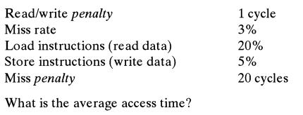
Suppose a unified cache has the following characteristics: Read/write penalty Miss rate Load instructions (read data) Store instructions (write data) Miss penalty What is the average access time? 1 cycle 3% 20% 5% 20 cycles
A 64-bit processor has a 8-MB, four-way setassociative cache with 32-byte lines. How is the address arranged in terms of set, line, and offset bits?
A computer with a separate data cache has a writeback cache memory. Cache line size is 64 bytes. Read access accounts for 80% of memory traffic. The processor, memory, and data buses are all 64-bits wide. Main memory latency (first access) is 20 cycles, and successive accesses take two cycles. The
There are three causes of cache miss: compulsory, capacity, and conflict. Define the meaning of these terms. Briefly explain what can be done to minimize their effect.
Why is memory management necessary in a system that uses hard disks?
What forms of protection can memory management provide?
Memory management has a protection function. Does such a facility exist with cache memory?
What are the fundamental differences between cache memory (as found in a CPU) and cache memory found in a hard disk drive?
What are the differences between write-back and write-through caches, and what are the implications for system performance?
A computer with a 32-bit address architecture has a memory management system with single-level 4 KB page tables. How much memory space must be devoted to the page tables?
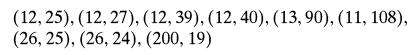
Consider a fully associative 16-byte cache with four lines of four words. The cache uses a LRU (least recently used) algorithm to deal with line replacement. When the cache is initially empty, lines are added from line 0 onward.Given the following sequence of hexadecimal addresses, indicate whether
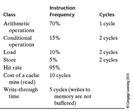
A computer runs an instruction set with the characteristics in the following table. What is the average number of cycles per instruction? Class Arithmetic operations Conditional operations Load Store Hit rate Cost of a cache miss (read) Write-through time Instruction Frequency 70% 15% 10% 5% 95%
Consider the following code that accesses three values in memory scalar integers x and s, and an integer vector y[i]. What is the memory latency in clock cycles for a trip round the loop ( after the first iteration)? Assume that the array is not cached and each new access to the array results in a
A 64-bit computer has a 128 KB 8-way associatively mapped cache. The cache has 128 sets and a line is 16 words. How many tag bits does each address require?
What type of cache is particularly useful in reducing thrashing in the cache due to repetitive swapping in and swapping out?
A 16-bit CPU has a cache with 32 lines, each of 16 bytes. The CPU accesses a byte at the decimal address 3210. This results in a miss and a line is loaded. Where is the line loaded in the cache?
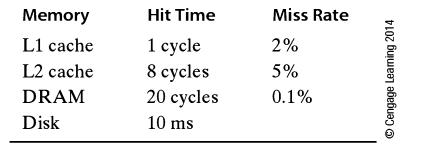
Given the following data and assuming a clock rate of 1,000 MHz. Calculate the average memory access time. Assume that L2 and DRAM are accessed in parallel with LL. Memory L1 cache L2 cache DRAM Disk Hit Time 1 cycle 8 cycles 20 cycles 10 ms Miss Rate 2% 5% 0.1% O Cengage Leaming 2014
Consider a computer with a 256-byte address space and a two-way 32-byte set associative cache. The computer word size is a byte, each cache line contains four bytes, and each cache four lines. If the cache is initially empty and the following sequence of hexadecimal addresses is read, show the
People are always looking for more effective cache mechanisms, particularly for ways of reducing the miss penalty (for example, using means of annex caches or victim caches). A student makes the following suggestion. Not all data is the same. Some numbers are used more frequently than others,
A computer has a cache with a hit ratio of 95% and a line size of four 32-bit words. The average processor cache access rate is 100 million/s. Twenty percent of CPU operations are loads/stores with 30% writes and 70% reads). The cache employs a write through mechanism and a line is replaced on a
Consider Problem 9.54 except that the cache uses a write-back mode. On average 25% of cache lines are dirty (have been modified).Data in Problem 9.54,A computer has a cache with a hit ratio of 95% and a line size of four 32-bit words. The average processor cache access rate is 100 million/s. Twenty
A computer has a 256 word memory and a 16 word cache. The cache line size is one word. The following sequence of addresses is read in series: Show how the cache memory would be accessed assuming that all lines are initially invalid. In each cache, mark the access as hit, capacity miss, compulsory
A computer with a 24-bit address bus has a main memory of size 16 MB and a cache size of 64 KB. The word length is two bytes.a. What is the address format for a direct-mapped cache with a line size of 32 words? b. What is the address format for a fully associative cache with a line size of 32
A system has a memory access time of 50 ns and a cache access time of 2 ns. The instruction time is 4 ns (not counting memory access) and the average instruction requires 0.25 memory accesses. If the hit rate is 0.90, what is the average instruction time?
Why is the hit rate of an L2 cache usually lower than that of an Ll cache?
A computer has a memory access time of 38 ns and does not use cache. Cache with an access time of 10 ns is added. The computer then runs 90% faster. Estimate the hit ratio.
A system has an L1 cache with a hit rate of 87% (hits takes one cycle). The L2 cache has a hit rate of 90% and a penalty of 10 cycles. The main store has an access time of 200 cycles. What is the average access time?
What is the meaning of the following terms (when applied to memory systems technology) ? a. Random access b. Serial access c. Dynamic RAM d. Static RAM e. Read-mostly memory f. Access time g. Non-volatile memory h. Cycle time
A computer has a memory space of 1 MB. a. How many address lines are required to span this address space, assuming it is byte-addressed? b. If this computer has a 16-bit data bus and can access bytes and 16-bit words, suggest ways in which the byte/word selection may take place. c. This computer
What is the meaning of memory hierarchy, and why is this concept of importance to the designer of PCs and similar workstations?
A memory component spans the address range 0x00400000 to 0x007FFFFF. What is its capacity?
At the beginning of this chapter, we stated that volatile read-only memory was an oxymoron. However, there is one application where a volatile read-only memory might be very beneficial under certain conditions. Can you think what this application might be?
A designer can use two different static memory devices to construct a computer with a 16-bit CPU. Both memory chips can hold 222 bits. Suppose it is necessary to construct a computer with a 16-bit data bus and 128 MB of storage. The memory chip is available as 256K words of 16 bits or 4 M words of
A company designs a computer in 2012. At its launch, the memory is twice as fast as the CPU. It is estimated that each year the CPU will get faster by 20%. Equally, it is estimated that each year the memory will get faster by 10%. After how many years will the CPU have to wait for the memory to
Why is all ROM RAM but not all RAM ROM?
Why is static RAM more suited to cache memory than DRAM?
What is the typical amount of main store, cache, and hard disk provided by current high-performance, state-of-the-art, cutting-edge personal computers?
We state that a static memory cell requires at least four transistors and a DRAM cell can use one transistor per bit. Could a memory ever use less than one transistor per bit to store data? Can you imagine a mechanism that could store more than one transistor per bit?
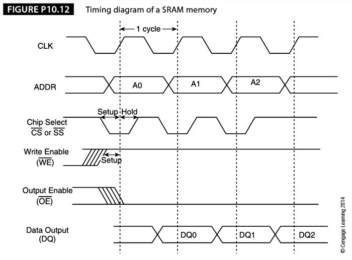
Given the timing diagram in Figure P10.12 that is derived from the data sheet of a commercial SRAM, explain its action in words. FIGURE P10.12 CLK ADDR Chip Select CS or SS Write Enable (WE) Output Enable (OE) Data Output (DQ) Timing diagram of a SRAM memory -1 cycle Setup Hold TILL'S AO Setup A1
Why does a DRAM have fewer pins (1/0 connections) than a static RAM of the same size (i.e., capacity in bits)?
In a conventional DRAM, what is the function of the column address and row address strobes?
In the context of DRAM timing, what is a pseudo maximum? What DRAM parameter is a pseudomaximim? What are the implications of a pseudo maximum for design engineers?
What fundamental properties of matter are exploited to implement memory systems? Can you think of any properties that have not yet been exploited and suggest ways in which they may be used to construct memory systems in the future?
What are the differences between Ovonic and ferroelectric memories?
A DDR SDRAM module in a PC is clocked at 133 MHz and is interfaced to a 64-bit data bus. What is the designation of the memory system in terms of the PCxx00 standard?
The speed of DRAM is increasing by about 7% a year, while the performance of processors is increasing by about 60%. What is the consequence of this state of affairs in the short term? What is the consequence in the long term?
You have a microprocessor chip with a 16-bit data bus. The computer accesses words; that is, it performs only 16-bit reads and writes. You are going to build a minimal computer which requires the processor and two 8-bit memory components. Unfortunately, you have only one 8-bit memory component,
A computer has a 64-bit data word and a 32-bit address. Interleave addressing is used with four banks. The total amount of memory is 1,024 MB. Show how the processor's 32-address bits are partitioned (i.e., divided into four fields).
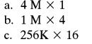
A computer with a 64-bit data bus uses the following memory chips. In each case, the chip is specified by locations X data width. For each of these chips, state the minimum number of chips required and the size of the corresponding memory block. a. 4 M X 1 b. 1 M X 4 c. 256K X 16
A DDR3 DRAM is specified as 9-9-9-24. What does this mean?
Suppose you could include cache memory in DRAM chips. How would you organize it, and what would the advantages be? What changes might have to be made to the computer system architecture?
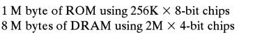
A CPU with a 24-bit address bus and 16-bit data bus implements the following memory blocks: Design an address decoder to implement this arrangement. 1 M byte of ROM using 256K X 8-bit chips 8 M bytes of DRAM using 2M X 4-bit chips
It has been reported that flash memory was reaching the limit of its density. Why do you think that this may be so?
What is wear leveling, and why does it have to be undertaken?
You have been asked to design the on-board computer for a deep-space vehicle. What special considerations would you have to take into consideration, and how would these affect your design?
What limits the areal density of a hard disk drive?
This chapter refers to an article on magnetic storage in the December 2000 edition of / EEE Spectrum with the title "Magnetic Storage: The medium that wouldn't die. " The title implies th at magnetic storage should have become obsolete. Explain why many may have believed this, and why magnetic
Explain the following terms as they are applied to magnetic storage technology. a. Domain b. Permeability c. M agnetostriction d. Remnant field e. Ferromagnetic f. Curie temperature g. Hard h. Soft
What are the major obstacles faced by the designer of hard drives?
Making hard drives for laptops and portable computers imposes a different set of design criteria on the engineer. What are the special considerations that the designer of mobile hard disks has to contend with ?
Hard disk drives once used combined inductive read/ write heads. Today, high-performance drives have GMR read heads. a. What is a GMR read-head? b. What are the advantages of separate read and write he ads?
Why is it difficult to fully erase data from a magnetic medium such as tape or disk?
Why does data have to be encoded before it can be written to a disk?
The following data sequence is to be MFM encoded for recording on a diskette. Draw the resulting waveform that would be presented to the write head. 0101001100001111
What are the criteria that determine the optimum size of a sector? Are these criteria permanent or do they change with time? What other developments in computing affect the answer to this question?
A hypothetical disk drive had the following parameters. The seek time for a short seek is given as 1 + 0.2Jn ms, and the seek time for a long seek is 3 + 0.003n ms. Assume that short seeks are less than 200 tracks.Suppose the drive accesses the following track numbers sequentially. What is the
A hard disk has the following parameters. • 6 surfaces • 20K tracks per surface • 256 sectors per track • 512 bytes per sector • Rotational speed 7,200 rpma. What is the capacity of the drive? b. What is the rotational latency? c. Once a sector has been accessed, what is the rate
How can disk drives be made faster (i.e., what options are available to the manufacturer)?
Describe the following disk head scheduling algorithms: FIFO, SSTF, SCAN, and C-SCAN.
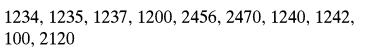
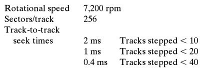
A hypothetical disk drive has the following properties. What is the approximate time required to access the following sectors, assuming that a new seek is not required if successive sectors are on the same track and the difference between sector numbers is greater than 1? The following data is
What is SMART technology, and how can it help the corporate hard disk user?
Showing 200 - 300
of 1390
1
2
3
4
5
6
7
8
9
10
11
12
13
14
Step by Step Answers
![tave Finternal teyc + Fmemory[ht + (1 - h)(te + ta)] teye where Finternal F memory fraction of time spent](https://dsd5zvtm8ll6.cloudfront.net/images/question_images/1705/9/1/0/76765ae21ef10d621705910767575.jpg)
![for (i = 0; i < 100; i++) { X = y [i]; S = S + X; }](https://dsd5zvtm8ll6.cloudfront.net/images/question_images/1705/9/1/5/36465ae33e4733451705915364081.jpg)