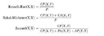
All Matches
Solution Library
Expert Answer
Textbooks
Search Textbook questions, tutors and Books
Oops, something went wrong!
Change your search query and then try again
Toggle navigation
FREE Trial
S
Books
FREE
Tutors
Study Help
Expert Questions
Accounting
General Management
Mathematics
Finance
Organizational Behaviour
Law
Physics
Operating System
Management Leadership
Sociology
Programming
Marketing
Database
Computer Network
Economics
Textbooks Solutions
Accounting
Managerial Accounting
Management Leadership
Cost Accounting
Statistics
Business Law
Corporate Finance
Finance
Economics
Auditing
Ask a Question
AI Study Help
New
Search
Search
Sign In
Register
study help
business
principles algorithms and systems
Questions and Answers of
Principles Algorithms And Systems
3. Suppose the page size in a paging system is 512 bytes. (a) If most of the files are large—that is, much greater than 512 bytes—what do you suppose is the average internal fragmentation(in
4. A computer has 12-bit addresses and a main memory that is divided into 16 frames. Memory management uses demand paging. *(a) How many bytes is virtual memory? (b) How many bytes are in each page?
5. Answer Exercise 4 for a computer with n-bit addresses and a memory divided into 2k frames.
6. For which pages in Figure 9.12 is the image on disk an exact replica of the page in main memory?
7. Verify the data of Figure 9.15(b), which shows Bélády’s anomaly, for the sequence of page references given in the text. Display the content of the frames in the format of Figure 9.13.
8. Devise a sequence of 12 page references for which the FIFO page-replacement algorithm is better than the LRU algorithm.
9. Plot the graph of Figure 9.15(b) for the page reference sequence in Figure 9.13 using the FIFO page-replacement algorithm. On the same graph, plot the data for the LRU algorithm.
10. If the operating system could predict the future, it could select the replacement page such that the next page fault is delayed as long as possible. Such an algorithm is called OPT, the optimum
11. Suppose a disk rotates at 5,400 revolutions per minute and has each surface divided into 16 sectors. *(a) What is the maximum possible latency time? Under what circumstance will that occur? (b)
12. (a) How many data bits are required to store one of the decimal digits 0 through 9? *(b)How many parity bits are required to detect a single error? (c) Write a single-error detection code using
13. (a) What must the code distance be to detect five errors? (b) What must the code distance be to correct five errors?
14. (a) Which entries in Figure 9.24 represent perfect codes? (b) Augment the table in Figure 9.24 with additional entries to include all the perfect codes between m = 4 and m = 128. Be sure to
15. (a) How many data bits are required to store one of the decimal digits 0 through 9? (b) How many parity bits are required to correct a single error? (c) Write a single-error correction code using
16. A set of eight data bits is transmitted with the single-error correction code of Figure 9.25.For each of the received bit patterns below, state whether an error occured. If it did, correct the
17. Figure 9.28 shows a RAID system with eight physical disks. (a) With six physical disks, how many mirror controllers and stripe controllers would you need for level 01 and for level 10?(b) With 2n
18. (a) Figure 9.28 shows the RAID level 01 and RAID level 10 systems with eight physical disks. Draw the equivalent systems for level 01 and level 10 with four physical disks. (b)Assume that two
19. You have a RAID level 4 system with eight data disks and one parity disk. (a) How many disk reads and disk writes must you make to write one data stripe if you do not make use of the old data and
1. (a) Prove the zero theorem x + 1 = 1 with Boolean algebra. Give a reason for each step in your proof. Hint: Expand the 1 on the left with the complement property and then use the idempotent
2. (a) Prove with Boolean algebra the absorption property, x + x · y = x. Give a reason for each step in your proof. (b) Show the dual proof of part (a).
3. (a) Prove with Boolean algebra the consensus theorem x · y + x′ · z + y · z = x · y + x′· z.Give a reason for each step in your proof. (b) Show the dual proof of part (a).
4. Prove De Morgan’s law, (a + b)′ = a′· b′, by giving the dual of the proof in the text. Give a reason for each step in your proof.
5. (a) Prove the general form of De Morgan’s law,(a1 · a2 · · · · · an)′ = a1′ + a2′ + · · · + an′ where n ≥ 2 from De Morgan’s law for two variables using mathematical
6. (a) Prove with Boolean algebra that (x + y) · (x′ + y) = y. Give a reason for each step in your proof. (b) Show the dual proof of part (a).
7. (a) Prove with Boolean algebra that (x + y) + (y · x′) = x + y. Give a reason for each step in your proof. (b) Show the dual proof of part (a).
8. *(a) Draw a three-input OR gate, its Boolean expression, and its truth table, as in Figure 10.10. (b) Do part (a) for the three-input NAND gate. (c) Do part (a) for the three-input NOR gate.
9. For each of the following Boolean properties or theorems, state the set theory interpretation:*(a) x + 0 = x(b) x · 1 = x(c) x + x′ = 1(d) x · x′ = 0(e) x · x = x(f) x + x = x(g) x · 0 = 0
10. (a) Show the associative property for the OR operation using Venn diagrams with x, y, and z overlapping regions. Sketch the following regions to show that region (3) is the same as region (6):(1)
11. (a) Show the distributive property using Venn diagrams with x, y, and z overlapping regions.Sketch the following regions to show that region (3) is the same as region (6):(1) x(2) y · z(3) x + y
12. (a) Show De Morgan’s law using Venn diagrams with a and b overlapping regions. Sketch the following regions to show that region (2) is the same as region (5):(1) a · b(2) (a · b)′(3)
13. Although a Boolean variable for a combinational circuit can have only two values, 1 or 0, Boolean algebra can describe a system where a variable can have one of four possible values—0, 1, A, or
14. The exclusive NOR gate, written XNOR, is equivalent to an XOR followed by an inverter. *(a) Draw the symbol for a two-input XNOR gate. (b) Construct its truth table. (c) The XNOR is also called a
15. Draw the nonabbreviated logic diagram for the following Boolean expressions. You may use XOR gates.*(a) ((a′)′)′*(b) (((a′)′)′)′(c) a′b + ab′(d) ab + a′b′(e) ab + ab′ +
16. Draw the abbreviated logic diagram for the Boolean expressions of Exercise 15. You may use XOR gates.
17. Construct the truth tables for the Boolean expressions of Exercise 15.
18. Write the Boolean expressions for the logic diagrams of FIGURE 10.63 . FIGURE 10.63 The logic diagrams for Exercise 18. b 300 (a) a (c) (b)
19. Write the Boolean AND-OR expression for the following:*(a) function y in Figure 10.3(b) function y in Figure 10.4(c) function x in Figure 10.17(d) the NAND gate in Figure 10.7(a)(e) the XOR gate
20. Write the Boolean OR-AND expression for the following:*(a) function y in Figure 10.3(b) function x in Figure 10.17(c) the NOR gate in Figure 10.7(b)(d) the XOR gate in Figure 10.7(c)
21. Use the properties and theorems of Boolean algebra to reduce the following expressions to AND-OR expressions without parentheses. The expressions may not be unique. Construct the truth table,
22. Construct two-level circuits for the expressions of Exercise 21 using only NAND gates.
23. Use the properties and theorems of Boolean algebra to reduce the following expressions to OR-AND expressions. The expressions may not be unique. Construct the truth table, which will be unique,
24. Construct a two-level circuit for the expressions of Exercise 23 using only NOR gates.
25. Draw the logic diagram of a two-level circuit that produces the XOR function using the following:*(a) only NAND gates(b) only NOR gates
26. State whether each gate in FIGURE 10.64 is the following:(1) an AND gate(2) an OR gate(3) a NAND gate(4) a NOR gate FIGURE 10.64 The gates for Exercise 26. (a) (b) D- (c) (d)
27. Write each function of Exercise 21 with the sigma notation.
28. Write each function of Exercise 23 with the pi notation.
29. In Figure 10.3, find the minimum AND-OR expression for the following:(a) x(a,b, c)(b) y(a,b, c)Draw the minimized two-level circuit for each expression with only NAND gates.
30. In Figure 10.3, find the minimum OR-AND expression for the following:(a) x(a,b, c)(b) y(a,b, c)Draw the minimized two-level circuit for each expression with only NOR gates.
31. Use a Karnaugh map to find the minimum AND-OR expression for x(a,b, c):(a) Σ(0, 4, 5, 7)(b) Σ(2, 3, 4, 6, 7)(c) Σ(0, 3, 5, 6)(d) Σ(0, 1, 2, 3, 4, 6)(e) Σ(1, 2, 3, 4, 5)(f) Σ(1, 2, 3, 4, 5,
32. Write each expression of Exercise 31 in pi notation. Use a Karnaugh map to find its minimum OR-AND expression.
33. Use a Karnaugh map to find the minimum AND-OR expression for x(a,b, c, d):(a) Σ(2, 3, 4, 5, 10, 12, 13)(b) Σ(1, 5, 6, 7, 9, 12, 13, 15)(c) Σ(0, 1, 2, 4, 6, 8, 10)(d) Σ(7)(e) Σ(2, 4, 5, 11,
34. Write each expression of Exercise 33 in pi notation. Use a Karnaugh map to find its minimum OR-AND expression.
35. Use a Karnaugh map to find the minimum AND-OR expression for x(a,b, c) with don’t-care conditions:*(a) Σ(0, 6) + d(1, 3, 7)(b) Σ(5) + d(0, 2, 4, 6)(c) Σ(1, 3) + d(0, 2, 4, 6)(d) Σ(0, 5, 7)
36. Use a Karnaugh map to find the minimum AND-OR expression for x(a,b, c,d) with don’tcare conditions:*(a) Σ(5, 6) + d(2, 7, 9, 13, 14, 15)(b) Σ(0, 3, 14) + d(2, 4, 7, 8, 10, 11, 13, 15)(c)
37. (a) A Karnaugh map for three variables has minterm 0 adjacent to 2, and 4 adjacent to 6.Copy Figure 10.30, cut out the Karnaugh map, and tape it in the shape of a cylinder so that adjacent
38. Using the viewpoint that one of the lines is a data line and the other is a control line, explain the operation of each of the following two-input gates:*(a) OR(b) NAND(c) NOR(d) XNOR See
39. Draw a nonabbreviated logic diagram of an eight-input multiplexer.
40. Construct a 16-input multiplexer from five 4-input multiplexers. Draw the 16-input multiplexer as a large block with 16 data lines labeled D0 through D15 and 4 select lines labeled S3 through S0.
41. Do Exercise 40 with two eight-input multiplexers without enable inputs and any other gates you need. Explain the operation of your circuit.
42. (a) Draw a nonabbreviated logic diagram of a 3 × 8 binary decoder. (b) Draw a nonabbreviated logic diagram of a 2 × 4 binary decoder with an enable input.
43. Construct a 4 × 16 binary decoder without an enable input from five 2 × 4 binary decoders with enable inputs. You may use the constant 1 as input to a device. Use the drawing guidelines of
44. Construct a 4 × 16 binary decoder without an enable input from two 3 × 8 binary decoders with enable inputs plus any other gates you need. Use the drawing guidelines of Exercise 40 to label
45. Implement the 2 × 4 binary decoder with an enable input, as shown in Figure 10.47. Draw a nonabbreviated diagram of your circuit.
46. *(a) Draw the implementation of the full adder in Figure 10.51 showing the AND and XOR gates of the half adders. *(b) What is the maximum number of gate delays from input to output? (c) Design
47. (a) Draw the circuit of Figure 10.52 with the individual XOR, AND, and OR gates of the half adders. *(b) What is the maximum number of gate delays from input to output? Consider an XOR gate as
48. Modify Figure 10.52(b) to provide two additional outputs, one for the N bit and one for the Z bit.
49. Implement a four-bit ASL shifter with select line S. The input is A3 A2 A1 A0, which represents a four-bit number with A0 the LSB and A3 the sign bit. The output is B3 B2 B1 B0 and C, the carry
50. Do Exercise 49 for a four-bit ASR shifter.
51. The block diagram in FIGURE 10.65 is a three-input, two-output combinational switching circuit. If s is 0, the input a is routed directly through to x, and b is routed to y. If s is 1, they are
52. The block diagram in FIGURE 10.66 is a four-input, two-output combinational switching circuit. If s1 s0 = 00, the a input is broadcast to x and y. If s1 s0 = 01, the b input is broadcast to x and
53. Draw the 12 two-input multiplexers of Figure 10.56. Show all the connections to the input and output lines. You may use ellipses (. . .) for 6 of the 8 data lines.
54. Implement the following logic units for the Pep/9 ALU:(a) logic unit 5, A · B(b) logic unit 6, A · B(c) logic unit 7, A ⊕ B(d) logic unit 8, A + B(e) logic unit 9, A ⊕ B(f) logic unit 10,
55. Draw the nonabbreviated implementation of the five-input, two-output control box of Figure 10.59. A7 B7 A6 B6 30 Sub A B A B A B Cout Cin Cout Cin Cout Cin S S S B Result e f g
18. A hexadecimal digit is '0'..'9', or 'a'..'f', or 'A'..'F'. A hexadecimal constant is a sequence of hexadecimal digits. Examples include 3,a, 0d, and FF4e. Use the direct-code technique for
17. Implement each FSM in Exercise 13 using the direct-code technique of the program in Figure 7.29. Write a procedure called parsePat() for a parse pattern that corresponds to parseNum(). Do not
16. Implement each FSM in Exercise 13 using the table-lookup technique of the program in Figure 7.28. Classify a character as B_ONE, B_ZERO, or B_OTHER in the transition table.
15. Improve the program in Figure 7.28 as suggested in the text by defining a third enumeration in Alphabet called T_OTHER, which represents a symbol that is neither a letter nor a digit.
14. Design a grammar that describes the source language of the translator in Figure 7.47.
12. Remove the empty transitions to produce the equivalent machine for each of the FSMs in FIGURE 7.52 .
11. For each of the machines shown in FIGURE 7.51 , (1) state whether the FSM is deterministic or nondeterministic, and (2) identify any states that are inaccessible.
8. For the grammar of Figure 7.8, draw the syntax tree for from the following strings, assuming that alpha, beta, and gamma are valid s and 1 and 24 are valids:*(a) alpha = 1 ;(b) alpha = alpha + 1
7. For the grammar of Figure 7.8, draw the syntax tree for from the following strings, assuming that S1, S2, S3, S4, C1, and C2 are valid s:*(a){ if ( C1 )S1 ;S2 ;}(b){ if ( C1 )if ( C2 )S1 ;else S2
6. For each of the following strings, state whether it can be derived from the rules of the grammar of Figure 7.5. If it can, draw the corresponding syntax tree:*(a) a + ( a )(b) a * ( + a )(c) a * (
5. Derive the following strings with the grammar of Figure 7.3:*(a) abc(b) aabbcc
4. Derive the following strings with the grammar of Figure 7.2 and draw the corresponding syntax tree:*(a) -d (b) +ddd (c) d
3. Derive the following strings with the grammar of Figure 7.1 and draw the corresponding syntax tree:(a) abc123(b) a1b2c3(c) a321bc
2. What is the identity element for the addition operation on integers? What is the identity element for the OR operation on Booleans?
1. What is the fundamental question of computer science?
24. Translate the following C program to Pep/9 assembly language. It multiplies two integers using an iterative shift-and-add algorithm.An iterative integer multiplication algorithm#include int
19. Assume you have a Pep/9-type computer and the following disk files:› File A: A Pep/9 assembly language assembler written in machine language› File B: A C-to-assembly-language compiler written
16. Write the program in Figure 4.35 in hexadecimal format for input to the loader. Verify that it works correctly by running it on the Pep/9 simulator with an input of up. Then modify the store byte
15. Write a machine language program to input two one-digit numbers, add them, and output the one-digit sum. There can be no space between the two one-digit numbers on input. Write the program in a
14. Write a machine language program to add the three numbers 2, –3, and 6 and output the sum on the output device. Store the –3 in hexadecimal. Do not use the subtract, negate, or invert
13. Write a machine language program to output the three characters Cat on the output device.Write it in a format suitable for the loader and execute it on the Pep/9 simulator.
12. Write a machine language program to output the four characters Frog on the output device.Write it in a format suitable for the loader and execute it on the Pep/9 simulator.
11. Write a machine language program to output your name on the output device. The name you output must be longer than two characters. Write it in a format suitable for the loader and execute it on
10. Suppose you need to process a list of 31,000 integers contained in Pep/9 memory at one integer per word. You estimate that 20% of the instructions in a typical program are unary instructions.
9. Determine the output of the following Pep/9 machine language program. The left column in each part is the memory address of the first byte on the line:*(a)0000 C1000A 0003 81000C 0006 F1FC16 0009
8. Determine the output of the following Pep/9 machine language program if the input is tab. The left column is the memory address of the first byte on the line:0000 D1FC15 0003 F1001F 0006 D1FC15
7. Determine the output of the following Pep/9 machine language program. The left column is the memory address of the first byte on the line:0000 D10013 0003 F1FC16 0006 D10014 0009 F1FC16 000C
6. Repeat Exercise 5 for the following statements:(a) C90A3F(b) D90A3F(c) F10A41(d) E10A41(e) 690A3F(f) 710A41(g) 890A3F(h) 990A3F(i) 06
Showing 100 - 200
of 532
1
2
3
4
5
6