All Matches
Solution Library
Expert Answer
Textbooks
Search Textbook questions, tutors and Books
Oops, something went wrong!
Change your search query and then try again
Toggle navigation
FREE Trial
S
Books
FREE
Tutors
Study Help
Expert Questions
Accounting
General Management
Mathematics
Finance
Organizational Behaviour
Law
Physics
Operating System
Management Leadership
Sociology
Programming
Marketing
Database
Computer Network
Economics
Textbooks Solutions
Accounting
Managerial Accounting
Management Leadership
Cost Accounting
Statistics
Business Law
Corporate Finance
Finance
Economics
Auditing
Hire a Tutor
AI Study Help
New
Search
Search
Sign In
Register
study help
engineering
fundamentals of solid state engineering
Questions and Answers of
Fundamentals Of Solid State Engineering
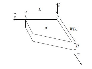
Consider the semiconductor block with a resistivity of 0.01 Ω.cm as shown in the figure below. The width of this block is constant but follows the relation W = 1 + 2(L - x) cm when x is varied from
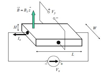
Consider the Hall effect measurement experiment depicted in the figure below. The dimensions of the semiconductor slab are L = 2 mm, W = 1 mm, and H = 2 μm. Assume the current Ix = 10 mA, the
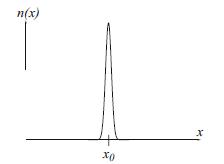
Consider an experiment where excess electrons are generated in a “burst” at t = 0 and x = x0 in a semiconductor, resulting in the concentration profile n(x) shown in the figure below.Draw the
The electron mobility in a Ge crystal is experimentally found to be proportional to T-1.66 (i.e., the mobility decreases with increasing temperature). Knowing that this mobility is 4000 cm2/Vs at 300
Consider an n-type Si semiconductor at room temperature with an excess electron concentration which decreases from 4 x 1016 cm-3 to 1 cm-3 (practically zero) over a distance of 1 mm. Determine the
A p-n junction diode has a concentration of NA = 1017 acceptor atoms per cm3 on the p-type side and a concentration of ND donor atoms per cm3 on the n-type side. Determine the built-in potential V0
A silicon p-n diode with NA = 1018 cm-3 has a built-in voltage of 0.814 eV and capacitance of 10 × 8 F.cm-2 at an applied voltage of 0.5 V. Determine the donor density. A = 1 cm2.
Plot the diode equation for an ideal Si p-n junction diode with an area 50 μm2, an acceptor concentration NA = 1018 cm-3, a donor concentration ND = 1018 cm-3, recombination lifetimes equal to τn =
Consider a Si p-n step junction with NA = 1017 cm-3 and ND = 1016 cm-3, with recombination lifetimes τp = 0.1 μs and τn = 0.01 μs and carrier mobilities μh = 450 cm2/Vs and μe = 800 cm2/Vs at
Determine the total reverse saturation current density, the reverse saturation current density due to holes and that due to electrons.
Assume a forward bias equal to V0/2 is applied, where V0, the built-in potential, is equal to 0.7546 V. Calculate the injected minority carrier currents at the edges of the space charge region.
Assume a reverse bias equal to -V0/2 is applied. Calculate the minority carrier currents at the edges of the space charge region.
With the help of Eq. (10.125), derive the magnetic field-dependent complex conductivity of an electron gas as given by Eq. (10.127):Discuss the behavior of the real part as a function of the magnetic
In your own words, explain how the multijunction cell illustrated works. How do the two absorbing junctions cooperate to optimize the collection of light over a wider spectrum?
Define the power collection efficiency Λ in terms of its components and explain why a square-shaped IV curve is better than a triangular one.
Let us assume a quantum dot which is spherical. The electrons or holes are confined at energy states with the following expression: Enl = (h2/2m∗)(αnl/R)2, where m* is the effective mass of the
Density of States of an Ideal Two-Dimensional Electron Gas Using the infinite barrier approximation, derive an expression for the density of states for electrons in a quantum well in terms of the
Fermi Energy of an Ideal Two-Dimensional Electron Gas Consider a structure consisting of two GaAs quantum wells that have been grown far apart in AlxGa1-xAs with the same Al composition x (x - 0.3).
The Graphic of the Two-Dimensional Density of States shows the density of states of a quantum well. The confinement energy of the lowest level (E1) is 17 meV, and the first excited state (E2) has a
The Moss-Burstein Shift in Absorption Spectra The “band filling” or Moss-Burstein shift effect occurs in all heavily doped three-dimensional semiconductors. It is a consequence of the fact that
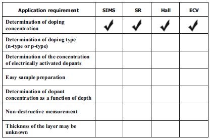
In this chapter we introduced four measurement techniques that yield the impurity concentration in semiconductor layers, namely, SIMS, sheet resistivity (SR) measurements, Hall effect measurements,
If the carrier collection efficiency is 1, what is the single most important factor which limits the solar cell performance in a single junction system?
Calculate the thermoelectric efficiency ZT for a device for which the conductivity is 105 siemens/cm, the thermal conductivity is κ = 5 W/Km, and the Seebeck coefficient α is 200 μV/kb, T = 300
(a) How does the spectrum of blackbody radiation scale with the temperature of a body? Make a typical sketch. (b) What is the photothermal effect? Explain how one can use the long-wavelength
Use your own ingenuity to design a thermoelectric material of high ZT. You can use any material and composition, drill holes, etc. Explain your choices. Plastic polymers are mechanically ideal, but
The Wiedemann-Franz law connects the thermal and electrical conductivity of a free electron gas in the Drude or nearly free electron gas approximation. The statement is (Eq. 6.38b):where κel is the
Explain what is meant by screening of electrical potentials. Explain the difference between the screening properties of metals and insulators. If in a solid the density of states at the Fermi level
What is a plasmon? What is the plasma frequency of a 3D metal for which the electron density is nc = 1027/m3. If you were asked to choose materials or design a system for which the plasmon frequency
Give an expression (an integral) for the total number of electrons in the conduction band of a bulk three-dimensional semiconductor and then in the first subband of a quantum well of width L in terms
A Si p-n junction is doped with an acceptor concentration NA = 5 × 1018 cm-3 and a donor concentration ND = 5 × 1015 cm-3. The critical electric field strength for breakdown is equal to 105
Consider an ideal metal-semiconductor junction between p-type silicon and polycrystalline aluminum. The Si is doped with NA = 5 × 1016 cm-3. The metal work function is 4.28 eV and the Si electron
Consider the same silicon-aluminum metal-semiconductor junction. The crosssectional area of the junction is 10 μm2. Assume that Be is 30 AK-2 cm-2 and the ideality factor n is 1. Calculate the
Calculate the real and imaginary part of the frequency-dependent admittance of a wire as a function of frequency, if the area is 1 cm2, the length 0.1 cm, the charge density 1021 cm-3, and the
Calculate the oscillator strength F12 linking the ground state n = 1 and first excited state n = 2 of box eigenstates with box size L = 1 nm and effective mass m* = 0.023 m0.
Calculate the reflectivity of a metal as a function of frequency using the Drude permittivity formula with free carrier concentration nc = 1022 cm-3, relaxation time τ = 10-12 s, and m* = 0.045 m0.
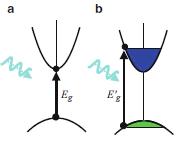
Explain the difference between direct and indirect bandgap materials. Sketch the two situations. If phonons were not allowed to provide the necessary momentum in an indirect bandgap excitation, what
Calculate the density of states per unit volume of a three-dimensional nearly free electron gas with effective mass m* in a magnetic field Bz perpendicular to the x-y plane including spin. Remember
What is meant by the permittivity of a solid? How is it calculated? How is it related to the refractive index? What does the real and imaginary part of the refractive index signify? How would you
The two-dimensional potential which confines the electrons in a quantum wire made of GaAs is assumed to be parabolic, and the subband separation is given as hω0 = 12 meV. If the Fermi energy is EF =
Critical Radius of a Spherical Quantum Dot with Finite Barrier Height Assume that a quantum dot has a spherical shape with radius R and is surrounded by a medium of higher bandgap such as AlGaAs. The
Explain what is meant by the electron-phonon interaction. Taking the one-dimensional diatomic chain treated in Chap. 6 as an example, illustrate with a simple diagram the difference between the
Derive the relation given in Eq. (17.3): aAxB1-xCyD1-y = xyaAC +x(1 - y)aAD + (1 -x)yaBC + (1 - x)(1 - y)aBD
Using the diagram in Fig. 17.1, graphically determine the compositions x and y of the quaternary alloy GaxIn1-xP1-yAsy which would yield a bandgap energy corresponding to the following wavelengths
Compare the MBE and MOCVD growth techniques, using a table that shows some of the advantages and disadvantages of each method.
Derive Eq. (17.8): Cs = kC0(1 - X)k - 1, where:Cs = impurity concentration in the solidC0 = original impurity concentration in the meltk = segregation coefficientX = fraction of the melt that has
Plot the dopant concentration profile of a 2000 long silicon rod grown by the floatzone technique using P as a dopant in a core doping scheme for various lengths of the floating zone. Assume the
Determine the growth rate of a layer grown by MOCVD using the following parameters:Diffusion coefficient (D) = 5 × 10⁻⁶ cm2.s-1 Thickness of the boundary layer (d) = 5 mm Surface reaction
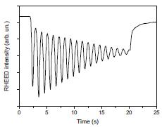
The figure represents the RHEED oscillation during homoepitaxy of GaAs in an MBE system.(a) At what moment did the growth start and stop?(b) What is the total thickness of GaAs material deposited?(c)
(a) Why does the amplitude of the oscillation slowly decrease with time in the figure of last problem? (b) Why does the RHEED intensity increase at the end of the curve?
In MBE, the deposition of AlxGa1-xAs is performed by opening simultaneously the Ga, Al, and As shutters.(a) Since, in normal growth conditions, the incorporation of Al and Ga atoms is unity, find an
The incident ion in an RBS measurement setup is 4He+ at E0 = 3 MeV. The angular position of the ion detector, θ, is chosen to be 170o. The backscattered beam from the surface of the sample under
In an RBS measurement setup, 4He+ at E0 = 2 MeV is used as incident ions. The scattering angle, θ, is 170o. The incident ions impinge on a 100 nm thick silicon sample (atomic mass of Si equals
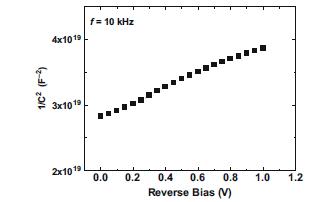
Estimate the acceptor concentration of the p-type GaN of Fig. 18.22. assuming a diode area of 400 μm × 150 μm and a dielectric constant of ε = 10ε0. f= 10 kHz 4x10¹⁹ 3x10¹⁹ 2x10 019 0.0
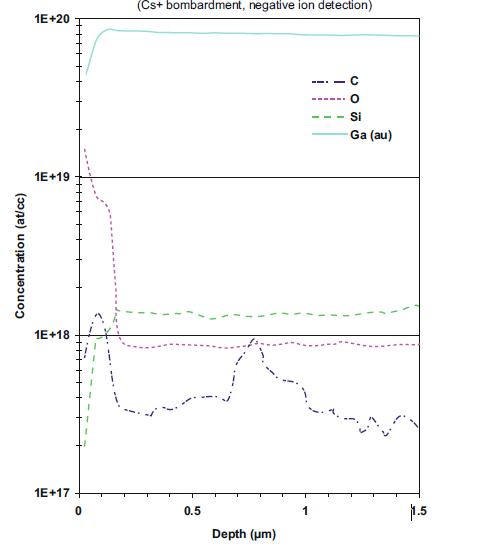
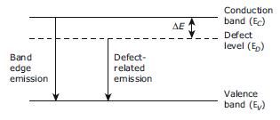
Based on the SIMS spectrum of Fig. 18.11:(a) Estimate the thickness of the oxide layer that has formed on the surface. (b) Si is an n-type dopant in the GaN material system. What is the
Based on the photoluminescence spectrum of Fig. 18.15: (a) Estimate the Al mole fraction (x) in the AlxGa1-xN layer. Assume that Vegard’s law holds for the calculation of the bandgap energy of
From the discussion of Rayleigh scattering, we recall that Rayleigh scattering is the elastic scattering of light off molecules that are smaller than the wavelength of that light. The intensity of
Do you think SEM and AFM are competing techniques or complementary techniques? Explain why.
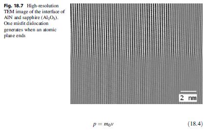
Based on the TEM image provided in Fig. 18.7, estimate the lattice mismatch between AlN and sapphire. Fig. 18.7 High-resolution TEM image of the interface of AIN and sapphire (Al,0,). One misfit
When an X-ray beam impinges upon a sample, it gets partially transmitted, partially absorbed, and partially scattered (diffracted). The ratio of the intensity of the transmitted beam to that of the
Give some examples of physical properties that defects can change.
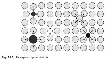
Identify the types of point defects shown in Fig. 19.1. Please re-sketch the figure. DO000000 OOQO 000000000 Fig. 19.1 Examples of point defects
Find the equilibrium concentration of defects for T = 0, 200, 400, 600, 800, 1000, and 1200 K if the energy to form a defect is 1 eV/atom. Assume A is unity. Graph your results. For T = 1200 K, how
The formation energies of vacancy clusters in Si are listed below. Calculate the formation energy of(i) system a (30 single vacancies),(ii) system B (five 6-vacancy clusters), and (iii) system C
Briefly describe the difference between an edge dislocation and a screw dislocation.
Show how to find the Burgers’ vector for a screw dislocation.
GaAs/InAs have a 7.2% lattice mismatch. How many monolayers of InAs may be grown on GaAs before a semi-coherent boundary is formed? (aGaAs = 0.565 nm aInAs = 0.606 nm, assume b = aInAs= √2).
What is preferential etching?
What have been the goals of the semiconductor industry in silicon crystal growth technology? Why?
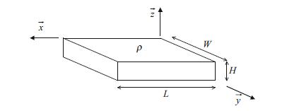
Consider the semiconductor slab shown in the figure below with dimensions L = 1 cm, W = 0.2 cm, and H = 0.25 cm and with a resistivity of 0.01 Ω.cm. What would be the resistance one would measure
Calculate concentrations of carriers in silicon doped by acceptors NA = 10 l4 cm-3 at:(a) 27 oC(b) 175 oC
Calculate the concentration of acceptor impurities in silicon, and determine the type of semiconductor, if at T = 300 K the concentration of electrons is 5 × 1011 cm-3 and the concentration of
Derive expressions for concentrations of free carriers in a semiconductor doped with both, donor and acceptor impurities. Determine the conductivity type and calculate the concentrations of carriers
Consider an n-type doped GaAs semiconductor at 300 K with an experimentally measured electron concentration of 3 × 1017 cm-3. The n-type dopant has an energy level such that ΔEd = EC = Ed = 25 meV.
Consider a p-type doped GaAs semiconductor at 300 K with an experimentally measured hole concentration of 1.5 × 1017 cm-3. The p-type dopant has an energy level such that ΔEa = Ea - EV = 125 meV.
Plot the evolution of the Fermi energy as a function of temperature in intrinsic GaAs.
Give an expression for the charge neutrality relation when double acceptors are present with a concentration NAA. Double acceptors accept one or two electrons. Use the same notations as those in
As we know P is an n-type dopant for Si and Ge. Nitrogen is in the same column as P in the periodic table. Will N be a good dopant? Why?
From the periodic table, give examples of n-type and p-type dopants for Ge and GaAs. Is silicon an n-type or a p-type dopant in GaAs? Interpret.
Calculate the intrinsic carrier concentrations for Si, Ge, GaAs, and GaN at 300 K, in the non-degenerate case. Plot their evolution as a function of temperature, in logarithmic scale.
Estimate relative errors in the calculation of free carrier concentration when the Maxwell-Boltzmann statistics is applied for semiconductors with Fermi energy within the energy gap, if the Fermi
Find the energies at which the distribution of electrons in the conduction band and the distribution of holes in the valence band have maxima, if distributions are governed by Maxwell-Boltzmann
Calculate the valence band effective density of states for Si, Ge, and GaAs at 300 K. Plot it as a function of temperature in logarithmic scale. We know that the valence band is degenerate at the
Calculate the conduction band effective density of states for Si, Ge, and GaAs at 300 K. Plot it in logarithmic scale as a function of the logarithm of the temperature.
Diamond is an electrical nonconductor; however, the thermal conductivity of diamond is greater than the thermal conductivity of copper for T > 40 K. How can this be explained?
In your own words, briefly describe the meaning of thermal conductivity and the physical processes that influence the thermal conductivity.
From the speed of sound equation, ν = (B/ρ)½, calculate the speed of sound in silicon and compare with the speed of sound in gallium arsenide. Assuming that the largest effect on the velocity
Look up in tables or reference books the room temperature lattice constants for the following crystals: aluminum, copper, iron, silicon, germanium, and diamond. Using the coefficients of linear
Let us model a rigid bar as a linear monatomic chain of atoms, as in Sect. 6.1.3 with the same notations. We further assume that the equilibrium interatomic separation is a and that its cross section
In your own words, describe the meaning of thermal expansion in solid-state engineering.
Plot the average number of phononsfor at least five values of T to show its evolution with increasing temperatures. For each one, plot the functionand show that it is a good approximation for N(ω)
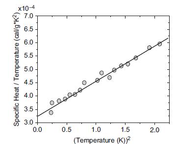
The figure below illustrates measurements of the specific heat (plotted as C/T versus T2) for a crystalline element. Use what you know about the origins and temperature dependence of the specific
From the figures for the phonon dispersion curves for Si and GaAs plus the equations for optical and acoustic phonons, explain why the energy for the Si curves is higher in energy than the curves for
The specific heat of metals is dominated by the electronic contribution at low temperatures and by phonons at high temperatures. At what temperature are the two contributions equal in rubidium? Note
Suppose that a light wave of wavelength 3 μm is absorbed by a one-dimensional diatomic harmonic chain with atoms of mass 4 × 10-26 kg and 5 × 10-26 kg and atomic spacing of 4.5 Å. What is the
It takes 450 cal to raise the temperature of a metallic sample from 20 to 35 C. What is the heat capacity of the metal sample? If the sample has a mass of 78 g, what is the specific heat of the
In Sect. 6.1.4, we calculated the ratio of the displacement amplitudes A and B for the long wave limit (k ! 0) for both the optical and acoustic phonon branches and then determined the displacement
Starting from the expression of the total energy carried by the lattice vibrations in Eq. (6.60), show that the heat capacity Cv = (dE/dT)v can be written as: T C, = 9Nk, Op (et – 1)2
Plot the shapes of the optical and acoustic branches in the dispersion relation for four different ratios of masses:and 1. Show that, in the case of two identical atoms, there is actually only one
In your own words, describe the meaning of heat capacity. How is heat capacity related to specific heat?
In the chapter, the phonon frequencies at the center of the zone k = 0 were determined for the diatomic molecule. Calculate the phonon frequencies at the zone boundary k = π/a.
Showing 1 - 100
of 165
1
2