All Matches
Solution Library
Expert Answer
Textbooks
Search Textbook questions, tutors and Books
Oops, something went wrong!
Change your search query and then try again
Toggle navigation
FREE Trial
S
Books
FREE
Tutors
Study Help
Expert Questions
Accounting
General Management
Mathematics
Finance
Organizational Behaviour
Law
Physics
Operating System
Management Leadership
Sociology
Programming
Marketing
Database
Computer Network
Economics
Textbooks Solutions
Accounting
Managerial Accounting
Management Leadership
Cost Accounting
Statistics
Business Law
Corporate Finance
Finance
Economics
Auditing
Hire a Tutor
AI Study Help
New
Search
Search
Sign In
Register
study help
sciences
digital systems design
Questions and Answers of
Digital Systems Design
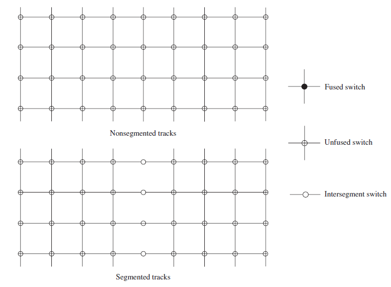
Route the “w”, “x”, “y”, and “z” nets on the segmented tracks shown in the diagram that follows. Use the minimum number of tracks possible.
In Question 9.24, it is assumed that data should be written into the register file during the write-back stage of an instruction before a subsequent instruction can read it. This introduces two idle
Perform a survey of FPGA chips now on the market.(a) Generate a table like Table 6-1 for current FPGAs.(b) Generate a table like Table 6-2 for current FPGAs.
Given the BILBO register that follows, specify B1 and B0 for each of the following modes:Normal modeShift register modePRPG (LSFR) modeMISR modeWhen in the PRPG mode, what sequence of states would be
(a) Write Verilog code for an 8-bit MISR that is similar to that shown in Figure 10-28.? (b) Design a self-test circuit, similar to that shown in Figure 10-25, for a 6116 static RAM. The write-data
Simulate the boundary scan tester of Figure 10-22 and verify that the results are as expected. Change the code to represent the case where the lower input to IC1 is shorted to ground; simulate again
Modern microprocessors employ pipelining to improve instruction throughput. Consider a 5-stage pipeline consisting of fetch, decode, and read registers along with execute, memory access, and register
(a) Some ISAs have byte-reversal instructions. Create an instruction that reverses the 4 bytes in one general-purpose register byte by byte and store it back to the destination register. Add this
(a) Some ISAs have bit-reversal instructions. Create an instruction that reverses the 32 bits in one general-purpose register bit by bit and store it back to the destination register. Add this
(a) Add overflow detection to all overflow-capable instructions in the MIPS subset that is implemented in Figure 9-8.(b) Write a test bench to test your code from part (a).
Figure 9.8 presents a model for a subset of MIPS instructions. Synthesize the model using current Xilinx software with a state-of-the-art Xilinx FPGA as the target. How many logic blocks, flip-flops,
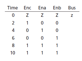
Based on the tri-state bus circuit (Figure 1-56), fill out the table that follows by using 4-valued logic. The values stored in RegA, RegB, and RegC are 8?d5, 8?d10, and 8?d15, respectively. Assume
What is the difference between $stop and $finish?
(a) Complete the following code by defining a macro Sum. Use parameters to initialize the numbers to 9 and 11.always @(posedge clk)begin$display("The sum of %d and %d is %d", A, B,
Indicate the final decimal value of the regA and regB after executing the following instructions.reg[8:0] regA;reg[8:0] regB;regA <= $unsigned -9;regB <= $signed 9'b100000000;
Write a task that logs the history of values of a bit vector signal to a text file. Each time the signal changes, write the current time and signal value to the file. Verilog has a built-in funtion
Write a task that has an integer signal and a file name as parameters. Each line of the file contains a delay value and an integer. The task reads a line from the file, waits for the delay time,
B is an integer array declared as integer B [4:0]. Write a Verilog code segment that will read five integers in a line of text from a file named “FILE2” and then write the five integers into
Create a 4 × 4 array multiplier using generate statements. Use full adder, half adder, and AND gate components.
The structural Verilog code that follows is a 2-input NOR gate with the rise/fall time defined as parameters.module NOR2(a, b, c);parameter Trise = 3;parameter Tfall = 2;parameter load = 1;input a,
Write structural Verilog code for a module that has two inputs: an N-bit vector A, and a control signal B (1 bit). The module has an N-bit output vector, C. When B = 1, C <= A. When B = 0, C is
Write structural Verilog code for a module that is an N-bit serial-in, serial-out rightshift register. Inputs to the shift register are bit signals: SI (serial input), Sh (shift enable), and CLK.
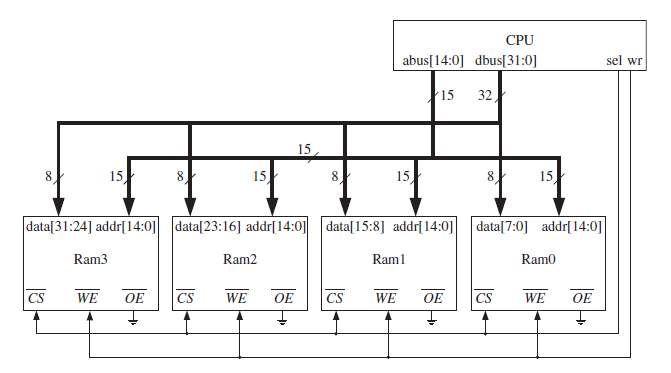
Four RAM memories are connected to CPU busses as shown here. Assume that the following RAM component is available.module SRAM(cs-b, we-b, oe-b, address, data);input cs-b,we-b,oe-b;input[14:0]
Write a Verilog model for an N-bit comparator using an iterative circuit. In the module, use the parameter N to define the length of the input bit vectors A and B. The comparator outputs should be EQ
(a) Write a model for a D flip-flop with a direct clear input. Use the following timing parameters: tplh(10 ns), tphl(10 ns), tsu(5 ns), th(3 ns), and tcmin(20). The minimum allowable clock period is
A clocked T flip-flop has propagation delays from the rising edge of CLK to the changes in Q and Q’ as follows: if Q (or Q’) changes to 1, tplh = 8 ns, and if Q (or Q’) changes to 0, tphl = 10
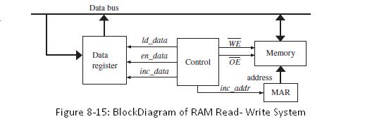
Design a memory tester that verifies the correct operation of a 6116 static RAM (Figure 8-15). The tester should store a checkerboard pattern (alternating 0s and 1s. ? ? ?K = 1 when counter is in
Design a memory-test system similar to that of Problem 8.18, except write a checkerboard pattern into memory (01010101 into address 0, 10101010 into address 1, etc.). Draw the block diagram and the
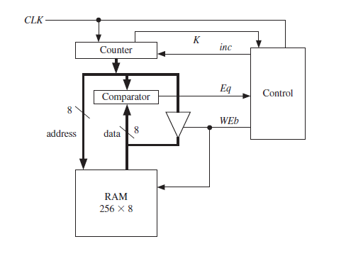
Design a memory-test system to test the first 256 bytes of a static RAM memory. The system consists of simple controller, an 8-bit counter, a comparator, and a memory as shown subsequently. The
In the following code, all signals are 1-bit. Draw a logic diagram that corresponds to the code. Assume that a D flip-flop with CE is available.assign F = (EA == 1) ? A: ((EB == 1)? B : Z);always
Write a Verilog function to compare two 8-bit vectors to determine whether they are equal. Report an error if any bit of either vector is not 0, 1, or z. The function call should pass only the
Write a Verilog module for one flip-flop in a 74HC374 (octal D-type flip-flop with 3-state outputs. Given the D-type flip-flop setup time = 15 ns, hold time = 5 ns, pulse width time = 15 ns). Assume
Write a Verilog module of an address decoder/address match detector. One input to the address decoder is an 8-bit address, addr. The second input is the 6-bit vector check. The address decoder will
A Verilog module has inputs A and B and outputs C and D. A and B are initially high. Whenever A goes low, C will go high 5 ns later, and if A changes again, C will change 5 ns later. D will change if
Write a Verilog user-defined primitive (UDP) for generating odd parity for 4-bit input data.
Create a user-defined primitive (UDP) for a J-K flip-flop with asynchronous clear and preset using “?” if needed
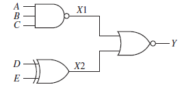
Write a Verilog model that uses only built-in primitives to implement the following circuit. Rise delay of NAND gate is 15 ns.Rise delay of XOR gate is 14 ns, fall delay of XOR gate is 16 ns.Rise
Hamming codes are used for error detection and correction in communication and memory systems. Error detection and correction capability is incorporated in these codes by inserting extra bits into
For the following Verilog code, list the values of B and C at each time a change occurs. Include all deltas and stop your listing when time > 8 ns. Assume that B is changed to 0110 at time 5 ns.
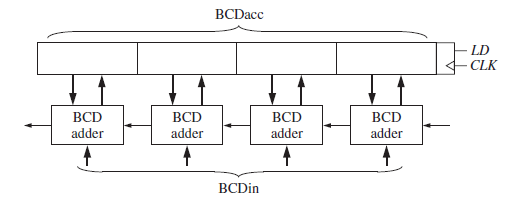
Write a Verilog module that implements a 4-digit BCD adder with accumulator (see the block diagram that follows). If LD = 1, then the contents of BCDacc are replaced with BCDacc + BCDin. Write a task
(a) Write a Verilog task that counts the number of 1s in an input bit vector that is up to N bits long (N ≤ 31). The output should be 5 bits long. The task call should have the following form: (N,
Write a Verilog module that could read numbers from a text file line by line and sort them by a user-defined task. The text file is named as “sort.txt”, which contains 10 positive integers. The
What are the major differences between Verilog functions and Verilog tasks?
The following Verilog code defines a function that computes the factorial of a number recursively. The automatic keyword is used to allow the function to be called recursively. Fill in the missing
(a) A and B are bit vectors that represent unsigned binary numbers. Write a Verilog function that returns TRUE (1) if A > B. The function call should be of the form GT(A, B, N), where N is the
a) Write a Verilog function that will create the 2’s complement of an N-bit vector. Use a call of the form comp2(bit_vec, N), where bit_vec is the vector and N is the length of the vector. Do the
Write a Verilog function to complete the following module, one that automatically counts the number of shifts. It needs to shift a word to the left until the most significant bit of the input word is
Assume that A, B, and C are floating-point numbers expressed in IEEE double precision floating-point format and that floating-point addition is performed.If A = 265, B = -265, C = 1, then(a)
Assume that A, B and C are floating-point numbers expressed in IEEE single precision floating-point format and that floating-point addition is performed.If A = 265, B = -265, C = 1, then(a)
Assume that A, B, and C are floating-point numbers expressed in IEEE double precision floating-point format and that floating-point addition is performed.If A = 240, B = -240, C = 1, then(a)
Assume that A, B, and C are floating-point numbers expressed in IEEE single precision floating-point format and that floating-point addition is performed. If A = 240, B = -240, C = 1,
Write a test bench for the floating-point adder of Figure 7-14.
This problem concerns the design of a digital system that converts an 8-bit signed integer (negative numbers are represented in 2’s complement) to a floating-point number. Use a floating-point
Synthesize the behavioral model of the 2’s complement multiplier (Figure 4-35) using whatever synthesis tool you have available. Then synthesize the model with control signals (Figure 4-40) and
Make any necessary changes in the Verilog code for the traffic light controller so that it can be synthesized without latches using whatever synthesis tool you have available. Synthesize the code
Assume that a sequential system with four states is to be implemented using a onehot state assignment, but the flip-flops do not have a preset input. The flip-flops do have a reset input; hence, it
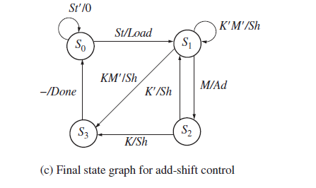
Make a one-hot state assignment for Figure 4-28(c). Derive the next-state and output equations by inspection. St' /0 K'M'/Sh St/Load S1 So KM'ISh M/Ad K'/Sh -/Done S2 S3 K/Sh (c) Final state graph
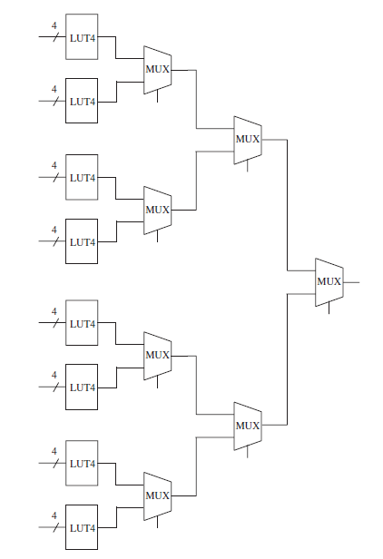
Indicate whether the following structure created using four slices from Xilinx SPARTAN FPGAs can implement each of the following (“All” means any of allpossible functions; “Some” means at
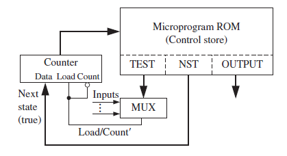
What are the conditions an SM chart must satisfy in order to realize it using single-address microprogramming with a counter, a ROM, and a multiplexer as in Fig 5-33?Figure 5-33: Microprogrammed
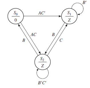
Make the necessary additions to the following state graph so that it is a proper, completely specified state graph. Demonstrate that your answer is correct. Convert the graph to a state table using
What does the term ISA mean? Do the Pentium 4 -> IBM POWER7 and Pentium 3 -> IBM POWER8 have the same ISA?
Microprocessor X has 30 instructions in its instruction set, and microprocessor Y has 45 instructions in its instruction set. You are told that Y is a RISC processor. Can you conclusively say that X
List four important characteristics that make a processor RISC type.
Compare the RISC ISA and the CISC ISA and list the benefits of each ISA. Which ISA will typically yield -> consume higher cycles per instruction (CPI)?
What is the difference between the MIPS addi instruction and the addiu instruction?
What is the difference between branch instructions and jump instructions?
What is the machine language encoding for the following MIPS instructions? Give the answers in hexadecimal (hex). All offsets are in decimal.(i) add $6, $7, $8(ii) lw $5, 4($6)(iii) addiu $3, $2,
What is the machine language encoding for the following MIPS instructions? Give the answers in hexadecimal (hex). All offsets are in decimal.(i) addi $5, $4 ,4000(ii) sw $5, 20($3)(iii) addu
What MIPS instruction do the following hexadecimal (hex) numbers correspond to? If it is not any instruction shown in Table 9-7, denote it as an illegal opcode.(i) 33333300(ii) 8D8D8D8D(iii)
What MIPS instruction do the following hexadecimal (hex) numbers correspond to? If it is not any instruction shown in Table 9-7, denote it as an illegal opcode.(i) 20202020(ii) 00E70018(iii)
Write a MIPS assembly language program for the following pseudocode segment:for(i = 0; i < 100; i++)x(i) = x(i) * y(i)
Write a MIPS assembly language program for the following pseudocode segment:for(i = 1; i < 100; i++)x(i) = x(i) + x(i-1)
Write a MIPS assembly language program for the following pseudocode segment:for(i = 0; i < 100; i++)y(i) = a * x(i) + y(i)
Write a MIPS assembly language program for the following pseudocode segment for matrix multiplication://The three matrices A, B, C are stored at 2000, 4000 and6000 respectivelyfor(i = 0; i < 3
(a) Figure 9-8 presents a model for a subset of MIPS instructions. Enhance the model by adding modules to interface the model to input switches and LEDs/ displays on an FPGA prototyping board. Your
Many microprocessors perform input-output operations by memory mapping. Assume that memory location F0002F2F is a parallel port for the processor. Write a MIPS program to generate a square wave with
(a) Add overflow detection to the add and addi instructions in the MIPS subset Verilog code (Figure 9-8).(b) Write a test bench to test your code from part (a).
(a) Add the MIPS instruction jal (jump and link) to the MIPS subset Verilog code (Figure 9-8). jal is used for procedure calls. jal jumpaddr puts the return address (PC + 1) in register file $31 and
(a) Add an instruction that multiplies two 16-bit numbers stored in the lower half of two general-purpose registers and deposits the product into another 32-bit register to the processor model shown
(a) Many ISAs have vector extensions where a 32-bit or 64-bit data is treated as four or eight smaller data elements (e.g., bytes or half-words). An add instruction then implicitly accomplishes four
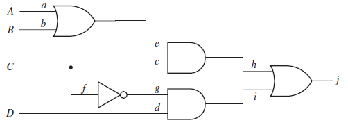
(a) Determine the necessary inputs to the following circuit to test for u stuck-at-0.(b) For this set of inputs, determine which other stuck-at faults can be tested.(c) Repeat (a) and (b) for r
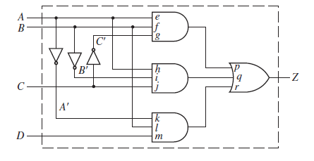
For the following circuit,(a) Determine the values of A, B, C, and D necessary to test for e s-a-1. Specify the other faults tested by this input vector.(b) Repeat (a) for g s-a-0. B ь
Find a minimum set of tests that will test all single stuck-at-0 and stuck-at-1 faults in the following circuit. For each test, specify which faults are tested for s-a-0 and for s-a-1. i
Give a minimum set of test vectors that will test for all stuck-at faults in the following circuit. List the faults tested by each test vector. D –
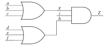
For the following circuit, specify a minimum set of test vectors for a, b, c, d, and e that will test for all stuck-at faults. Specify the faults tested by each vector. a b
For the following circuit, find a minimum number of test vectors that will test all s-a-0 and s-a-1 faults at the AND and OR gate inputs. For each test vector, specify the values of A, B, C, and D,
Find a test sequence to test for b s-a-0 in the sequential circuit of Figure 10-7.
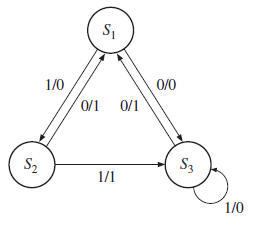
A sequential circuit has the following state graph:The three states can be distinguished using the input sequence 11 and observing the output. The circuit has a reset input, R, that resets the
State graphs for two sequential machines are given here. The first graph represents a correctly functioning machine, and the second represents the same machine with a malfunction. Assuming that the
When testing a sequential circuit, what are the major advantages of using scan-path testing as compared with applying input sequences and observing output sequences?
A scan path test circuit of the type shown in Figure 10-8 has three flip-flops, two inputs, and two outputs. One row of the state table of the sequential circuit to be tested is as follows:For this
(a) Redraw the code converter circuit of Figure 1-26 in the form of Figure 10-8 using dual-port flip-flops.(b) Determine a test sequence that will verify the first two rows of the transition table of
(a) Write Verilog code for a dual-port flip-flop.(b) Write Verilog code for your solution to Problem 10.12(a).(c) Write a test bench that applies the test sequence from Problem 10.12(b) and compare
Instead of using dual-port flip-flops of the type shown in Figure 10-8, scan testing can be accomplished using standard D flip-lops with a MUX on each D input to select D1 or D2. Redraw the circuit
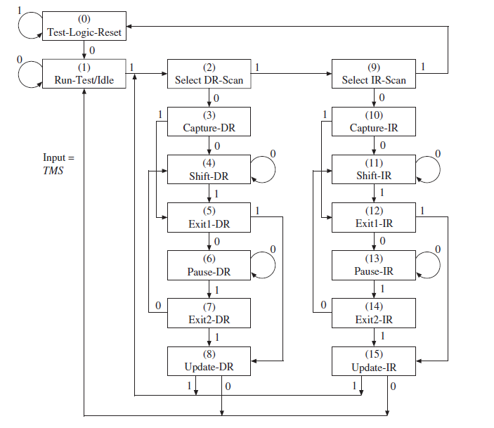
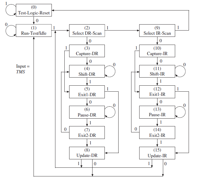
Referring to Figure 10-16, determine the sequence of TMS and TDI inputs required to load the instruction register with 011 and the boundary scan register BSR2 with 1101. Start in state 0 and end in
The INTEST instruction (code 010) allows testing of the core logic by shifting test data into the boundary scan register (BSR1) and then updating BSR2 with this test data. For input cells this data
Based on the Verilog code of Figure 10-21, design a 2-cell boundary scan register. The first cell should be an input cell, and the second cell an output cell. Do not design the TAP controller; just
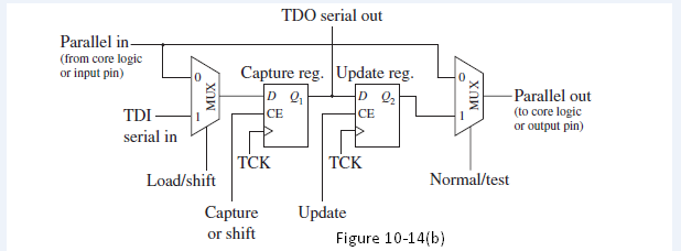
Write Verilog code for the boundary scan cell of Figure 10-14(b). Rewrite the Verilog code of Figure 10-21 to use this boundary scan cell as a component in place of some of the behavioral code for
(a) Draw a circuit diagram for an LFSR with n = 5 that generates a maximum-length sequence.(b) Add logic so that 00000 is included in the state sequence.(c) Determine the actual state sequence.
(a) Draw a circuit diagram for an LFSR with n = 6 that generates a maximum-length sequence.(b) Add logic so that 000000 is included in the sequence. (c) Determine the 10 elements of the sequence
Showing 1 - 100
of 323
1
2
3
4